Flexible 3-D Photonic Device

a photonic device and flexible technology, applied in the field of optical waveguides, can solve the problems of limited functionality of photonic waveguides fabricated using semiconductor wafers, and achieve the effect of increasing functionality

Active Publication Date: 2014-08-07
AMERICAN SEMICON
View PDF5 Cites 127 Cited by
  • Summary
  • Abstract
  • Description
  • Claims
  • Application Information

AI Technical Summary

Benefits of technology

[0004]Bonding a wafer or individual die from a III-V (GaAs, Gallium Arsenide, for instance) semiconductor (or similar photonic material) on to the flexible silicon prior to demount can create an active region for lasers, amplifiers, modulators, and other photonic devices using standard processing techniques on the pre-demount flexible substrates. Following demount, additional photonic devices may be mounted to the opposite side of flexible photonic waveguide structure for 3-D device stacking. Alternatively, multiple flexible photonic waveguides may be stacked to increase functionality with light transfer occurring between the stacked waveguides. The flexible photonic circuit allows for integration of photonic devices such as low threshold lasers, tunable lasers, and other photonic integrated circuits with flexible Complementary Metal Oxide Semiconductor (CMOS) integrated circuits.

Problems solved by technology

Present day photonic waveguides fabricated using semiconductor wafers are limited to routing light in two dimensions, that is, in x and y directions, within the plane of rigid crystalline silicon.

Method used


Image

  • Flexible 3-D Photonic Device
  • Flexible 3-D Photonic Device
  • Flexible 3-D Photonic Device

Examples


Embodiment Construction

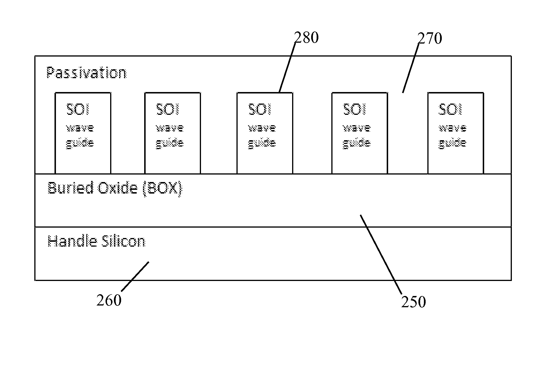
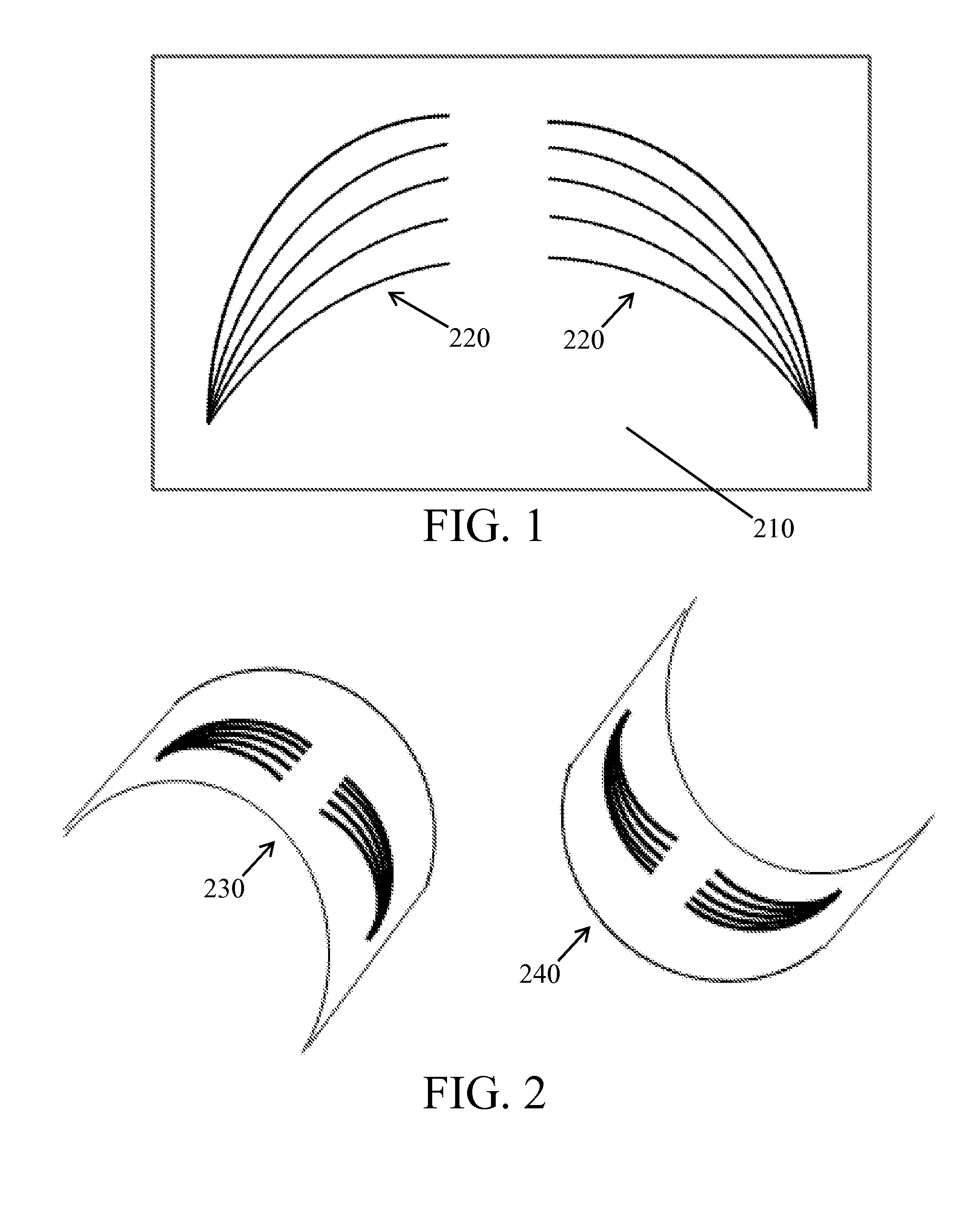
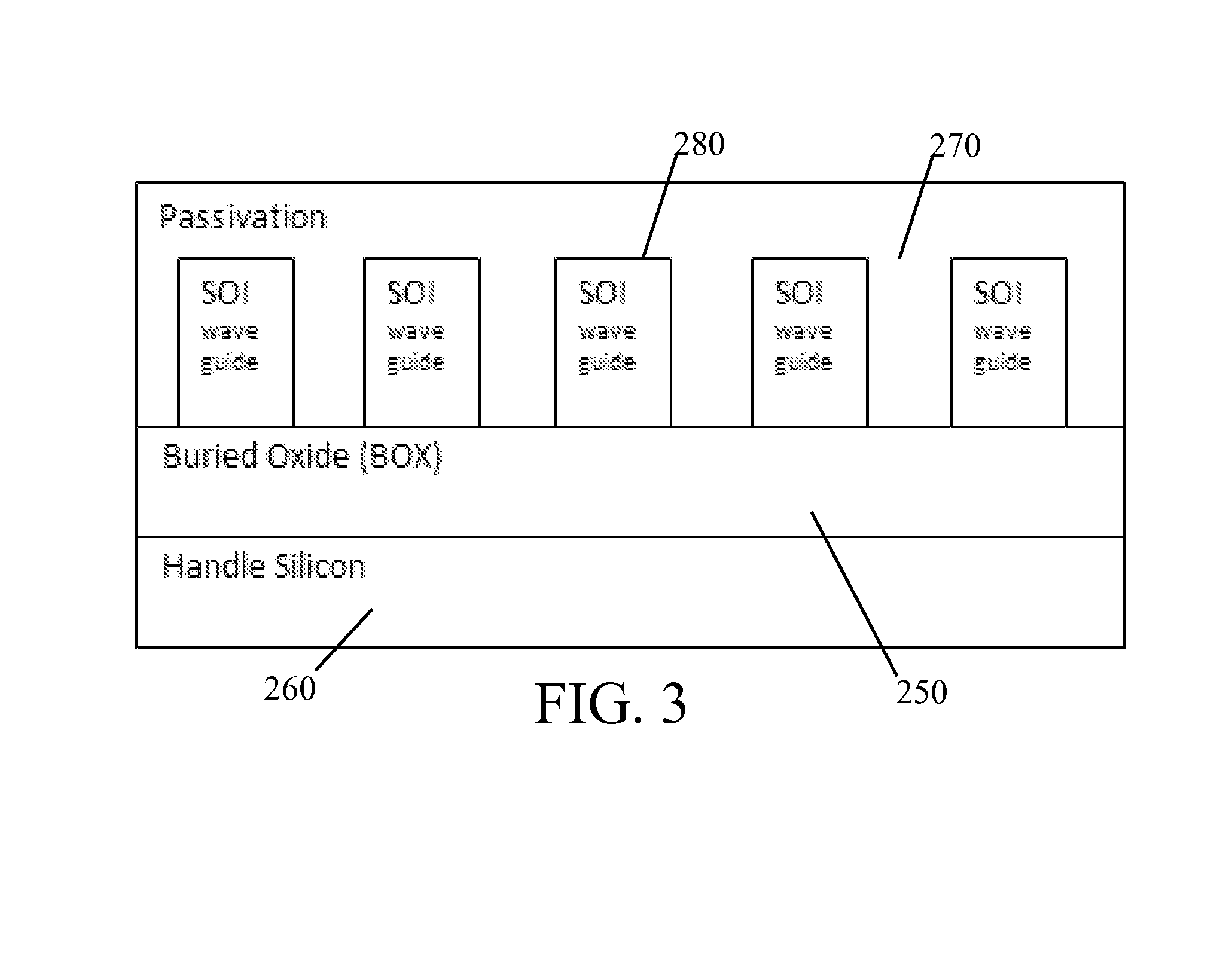
[0021]Ultra-small geometrical silicon photonic structures have been demonstrated as photonic waveguides. Integration of these waveguides with microelectronics provides a highly integrated platform for electronic-photonic convergence. The practical achievement of this platform requires reduction of such factors as the propagation and coupling losses in the interface to external fibers. State-of-the-art technologies specially tuned to the fabrication of nanometer structures, and the fundamental propagation performance has already become a practical standard. Some passive devices, such as branches and wavelength filters, and dynamic devices based on the thermo-optic effect or carrier plasma effect have been developed by using silicon photonic wire waveguides. These waveguides also offer an efficient media for nonlinear optical functions, such as wavelength conversion. Although polarization dependence remains a serious obstacle to the practical applications of these waveguides, waveguid...


PUM


Abstract

Three-dimensional flexible photonic integrated circuits on silicon are fabricated in semiconductor wafer form and then transferred to Silicon-on-Polymer (SOP) substrates. SOP provides flexibility for conformal mounting with devices capable of maintaining performance when dynamically deformed to allow routing of light in x, y and z directions. Bonding a wafer or individual die of III-V semiconductor, such as Gallium Arsenide or similar photonic material, to the flexible silicon creates an active region for lasers, amplifiers, modulators, and other photonic devices using standard processing. Mounting additional photonic devices to the opposite side of a flexible photonic waveguide produces a stack for three-dimensional devices. Multiple flexible photonic waveguides may be stacked to increase functionality by transferring light between stacked waveguides. The flexible photonic circuit allows for integration of photonic devices such as low threshold lasers, tunable lasers, and other photonic integrated circuits with flexible Complementary Metal Oxide Semiconductor (CMOS) integrated circuits.

Description

CROSS-REFERENCES TO RELATED APPLICATIONS[0001]Not applicableFIELD OF THE INVENTION[0002]The present invention relates generally to optical waveguides. In particular, the described devices are produced by standard semiconductor processing techniques on a flexible substrate.BRIEF SUMMARY OF THE INVENTION[0003]Present day photonic waveguides fabricated using semiconductor wafers are limited to routing light in two dimensions, that is, in x and y directions, within the plane of rigid crystalline silicon. By fabricating waveguides in a semiconductor wafer form and then converting those wafers to Semiconductor-on-Polymer (SOP), the waveguides can provide routing for light in x, y and z directions. The SOP format provides for sub-micron sized features that are flexible for conformal mounting or capable of maintaining performance while being deformed dynamically. The result is a fully flexible sub-micron feature-capable waveguide.[0004]Bonding a wafer or individual die from a III-V (GaAs, G...

Claims


Application Information

Patent Timeline
Patent Type & Authority Applications(United States)
IPC IPC(8): G02B6/12
CPCG02B6/12002G02B6/1221G02B6/122G02B6/13G02B2006/12061
Inventor HACKLER, SR., DOUGLAS R.WILSON, DALE G.
Owner AMERICAN SEMICON
Why Eureka
Try Eureka