

Flip-chip hybridization of microelectronic components using suspended fusible resistive connection elements
a technology of fusible resistive connection elements and flip-chips, which is applied in the field of flip-chip hybridization of microelectronic components, can solve the problems of settling the first component under its own weigh
- Summary
- Abstract
- Description
- Claims
- Application Information
AI Technical Summary
Benefits of technology
Problems solved by technology
Method used
Image

Examples
Embodiment Construction
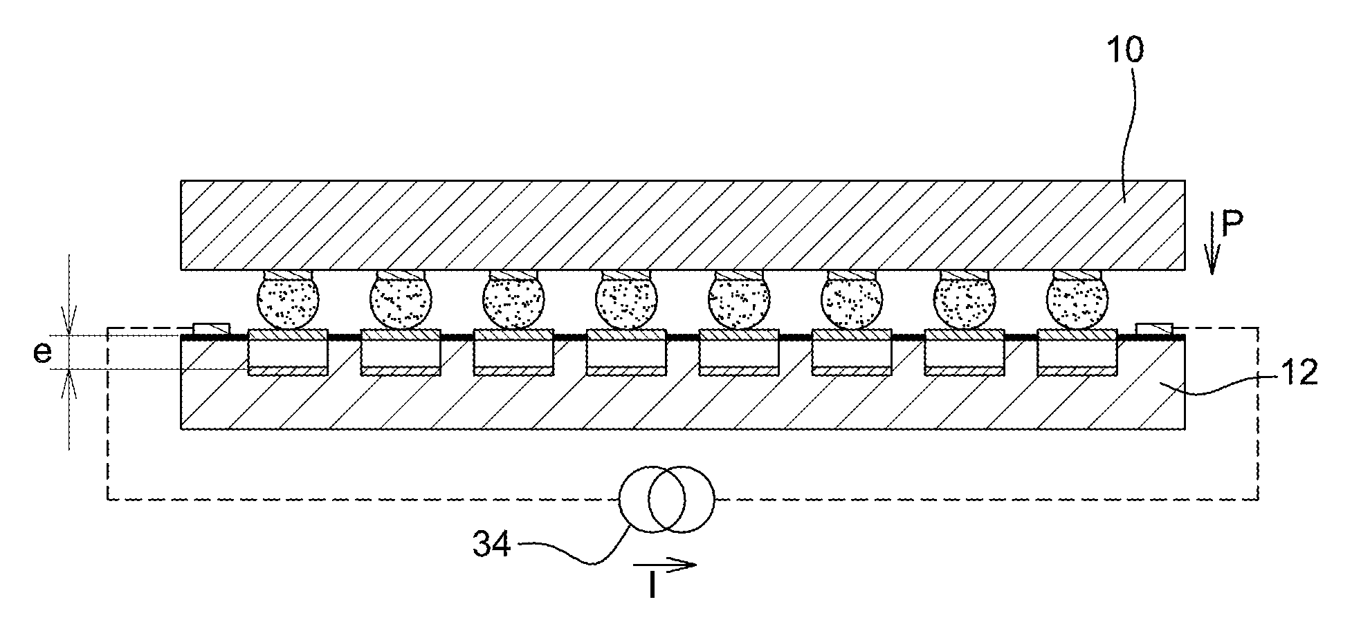
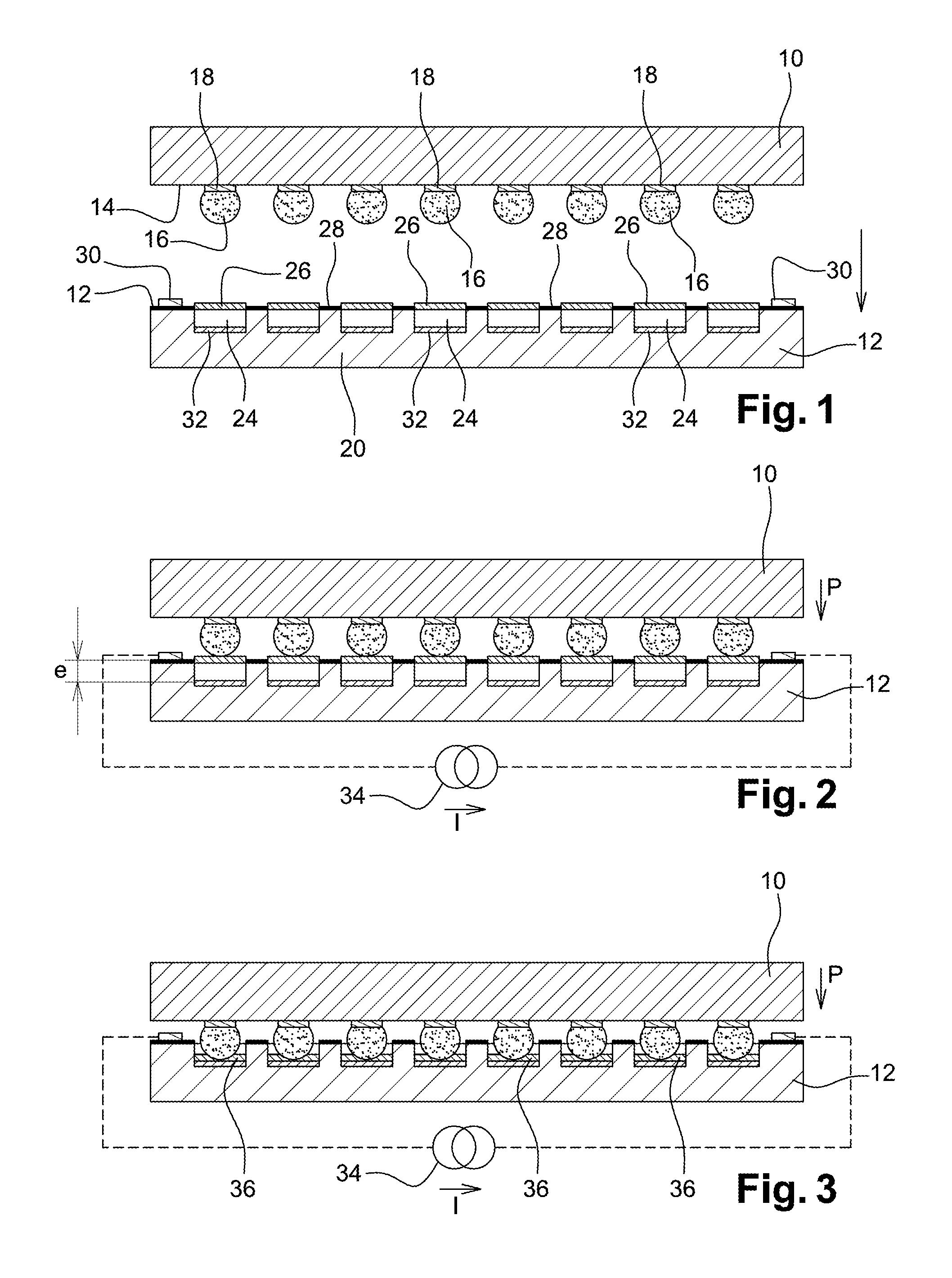
[0029]A method of hybridizing a first microelectronic component 10 with a second microelectronic component 12 according to the invention is now described in relation with the simplified cross-section views of FIGS. 1 to 3.
[0030]First microcomponent 10, for example, a silicon-based microelectronic chip comprises, on one of its surfaces 14, metal balls 16, for example, soldered to metal areas 18, as known per se in the state of the art.
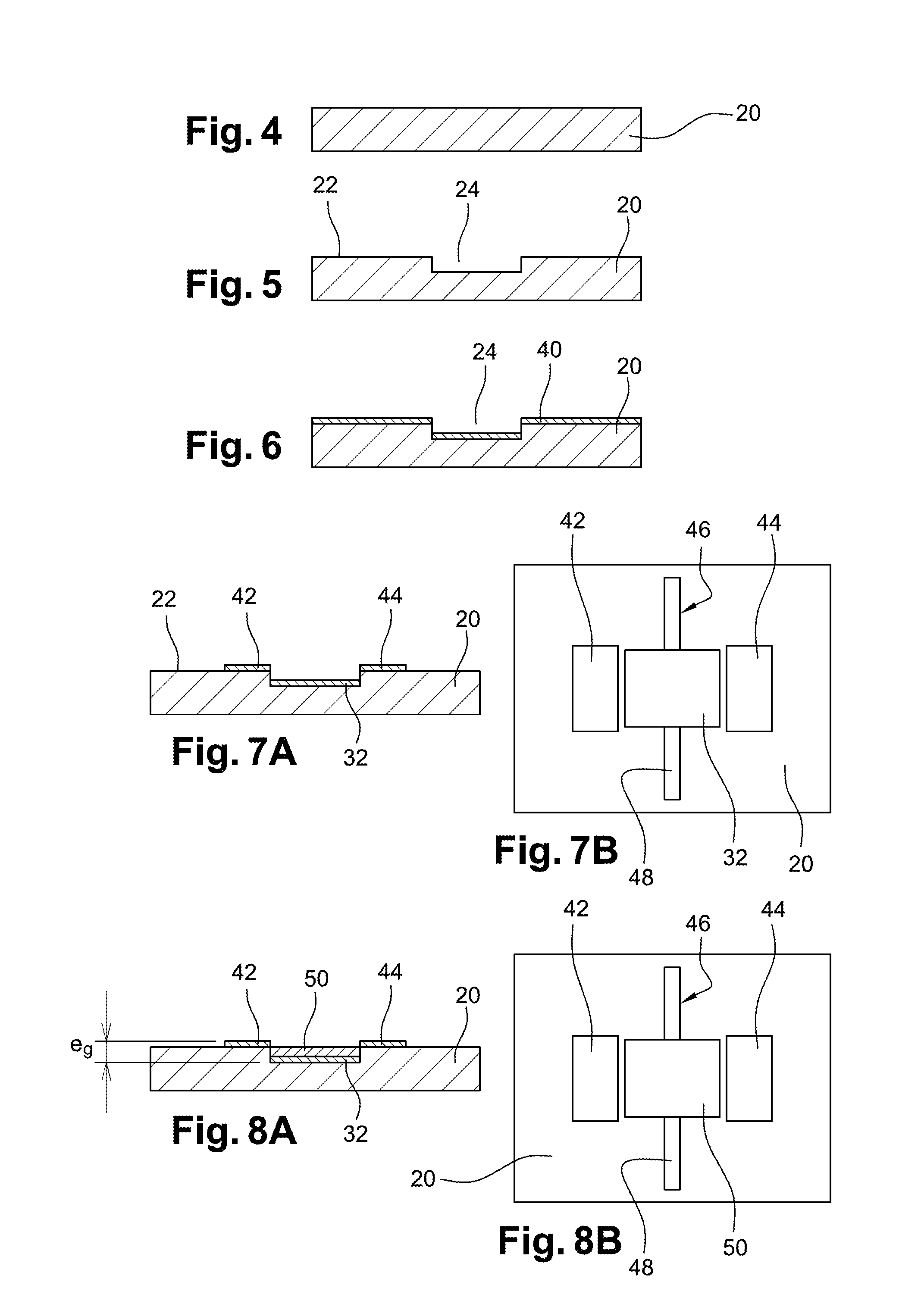
[0031]Second microcomponent 12 comprises a substrate 20, for example, a flexible plastic substrate, particularly made of PET or of PEN, in a surface 22 of which are formed cavities 24 intended to respectively receive balls 14 of first component 10.
[0032]A resistive element 26 made of a fusible material, for example, indium, or of an alloy of gold and tin, is further suspended above each cavity 24 and is connected, for example, via metal tracks 28 formed on surface 22 of second component 12, to electric power supply terminals 30, to enable the flowing of...
PUM
 Abstract
Description
Claims
Application Information