Semiconductor device

a technology of semiconductor devices and semiconductors, applied in the direction of semiconductor devices, electrical devices, transistors, etc., can solve the problems of limited operation at high temperature, difficult to achieve higher performance, and the performance of silicon power devices reaching their limit, so as to achieve high-resolution and high-resolution high-resolution results

Active Publication Date: 2014-08-14
SEMICON ENERGY LAB CO LTD
View PDF23 Cites 35 Cited by
  • Summary
  • Abstract
  • Description
  • Claims
  • Application Information

AI Technical Summary

Benefits of technology

[0020]According to the present invention, a semiconductor device that includes an oxide semiconductor and is suitable for a power device can be provided. Further, a semiconductor device in which large current can flow can be provided. Furthermore, a highly reliable semiconductor device can be provided.

Problems solved by technology

However, the performance of a power device including silicon is reaching its limit, and it is becoming difficult to achieve higher performance.
In the case where silicon is used for a power device, there is a limitation on operation at a high temperature because the band gap of silicon is small.

Method used


Image

  • Semiconductor device
  • Semiconductor device
  • Semiconductor device

Examples


embodiment 1

[0050]In this embodiment, a structural example of a semiconductor device of one embodiment of the present invention is described with reference to drawings. A transistor is described as an example of the semiconductor device.

Structural Example 1

Structure Example of Transistor

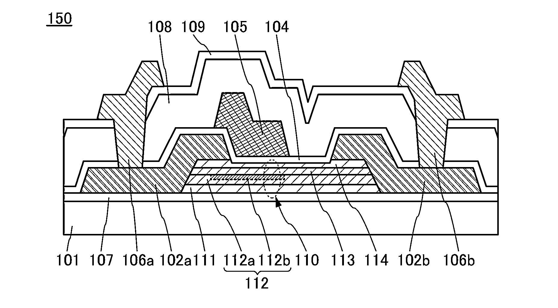
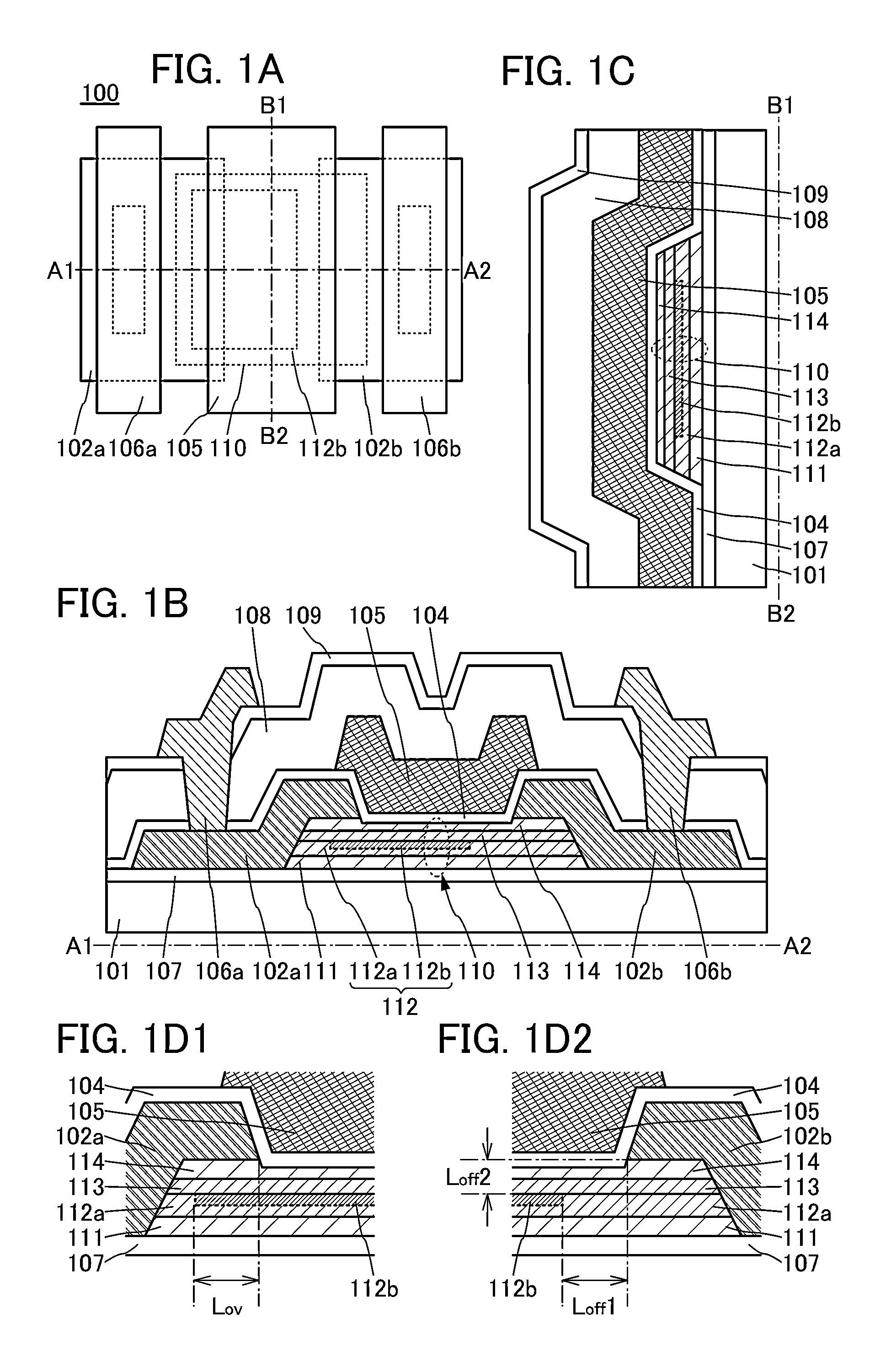
[0051]FIGS. 1A to 1D2 illustrate a transistor 100 that is an example described in this structural example. FIG. 1A is a schematic top view of the transistor 100. FIGS. 1B and 1C are schematic cross-sectional views taken along lines A1-A2 and B1-B2 in FIG. 1A, respectively. Note that FIG. 1A illustrates only main components for simplicity.

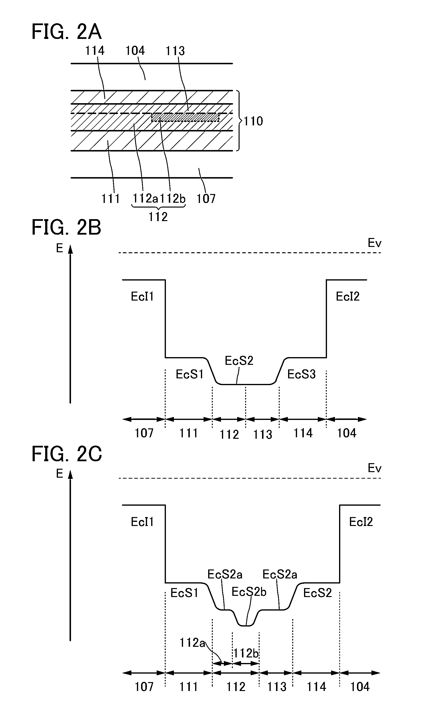
[0052]The structure illustrated in FIGS. 1A to 1D2 includes an oxide stack 110 which is provided over an insulating layer 107 provided over a substrate 101. The oxide stack 110 has a stacked-layer structure in which a first oxide layer 111, a first oxide semiconductor layer 112, a second oxide semiconductor layer 113, and a second oxide layer 114 are stacked in this order. A fir...

example 1

Manufacturing Method Example 1

[0234]An example of a method for manufacturing the semiconductor device of one embodiment of the present invention is described below with reference to drawings.

[Example of Method for Manufacturing Transistor]

[0235]Here, an example of a method for manufacturing the transistor 150 described in the above modification example is described. FIGS. 4A to 4D and FIGS. 5A to 5C are schematic cross-sectional views of the manufacturing process.

[Formation of Insulating Layer 107]

[0236]First, the insulating layer 107 is formed over the substrate 101.

[0237]As the substrate 101, a substrate which is resistant to heat in the manufacturing process is used. For example, a glass substrate, a metal substrate, an alloy substrate, a single crystal semiconductor substrate of silicon, silicon carbide, or the like can be used. Alternatively, a substrate in which a device such as another transistor is formed on the substrate 101 may be used. In this case, the device may be form...

modification example 1

[0305]An example of a method for manufacturing a transistor which is partly different from the example of method for manufacturing a transistor is described below. Note that different points from those described above are described below, and the common portions may be omitted.

[0306]First, in a manner similar to the above manufacturing method, the insulating layer 107, the first oxide layer 111, and the first oxide semiconductor layer 112 are formed over the substrate 101. Subsequently, the resist mask 121 is formed over the first oxide semiconductor layer 112. Then, the element 122 is introduced to part of the first oxide semiconductor layer 112 through an opening portion of the resist mask 121, so that the second region 112b containing the element 122 and the first region 112a having a low concentration of the element 122 are formed in the first oxide semiconductor layer 112 (see FIG. 6A).

[0307]After the introduction of the element 122, the resist mask 121 is removed.

[0308]Next, u...


PUM


Abstract

An object is to provide a semiconductor device that includes an oxide semiconductor and is suitable for a power device. An object is to provide a semiconductor device in which large current can flow. An object is to provide a highly reliable semiconductor device. A semiconductor device includes an oxide stack in which a first oxide layer, a first oxide semiconductor layer, a second oxide semiconductor layer, and a second oxide layer are stacked and has a structure in which a region that contains an element imparting conductivity and is provided in the first oxide semiconductor layer overlaps an electrode functioning as a source electrode and does not overlap an electrode functioning as a drain electrode.

Description

BACKGROUND OF THE INVENTION[0001]1. Field of the Invention[0002]The present invention relates to an object, a method, or a manufacturing method. In addition, the present invention relates to a process, a machine, manufacture, or a composition of matter. In particular, the present invention relates to, for example, a semiconductor device, a display device, a light-emitting device, a power storage device, a driving method thereof, or a manufacturing method thereof. The present invention particularly relates to a semiconductor device, a display device, or a light-emitting device each including an oxide semiconductor, for example.[0003]In this specification, a semiconductor device generally means a device which can function by utilizing semiconductor characteristics. For example, a semiconductor element such as a transistor; a power device; an integrated circuit, a power supply circuit, or a power supply converter circuit each including a power device; an electro-optical device; a semic...

Claims


Application Information

Patent Timeline
Patent Type & Authority Applications(United States)
IPC IPC(8): H01L29/786H01L29/24
CPCH01L29/24H01L29/7869H01L29/42384H01L29/4908H01L29/78606H01L29/78696
Inventor YAMAZAKI, SHUNPEISUZAWA, HIDEOMISHIMOMURA, AKIHISATANAKA, TETSUHIROTEZUKA, SACHIAKI
Owner SEMICON ENERGY LAB CO LTD
Why Eureka
Try Eureka