Wiring board and light emitting device using same, and manufacturing method for both

Inactive Publication Date: 2014-08-14
PANASONIC INTELLECTUAL PROPERTY MANAGEMENT CO LTD
View PDF0 Cites 9 Cited by
  • Summary
  • Abstract
  • Description
  • Claims
  • Application Information

AI Technical Summary

Benefits of technology

[0017]In the above configuration, the use of the plate wirings formed of the metal plates allows connecting the first top-surface wiring and the first bottom-surface wiring through a material having low electrical and thermal resistances. Furthermore, the plate wirings and the insulating portion are made to be substantially as thick as each other; therefore, the surface wirings electrically connected directly to the plate wirings can be formed with high accuracy. In addition, the surface wirings are thinner than the plate wirings, and the minimum wiring gap between the surface wirings is smaller than the minimum wiring gap between the plate wirings; therefore, the wiring patterns are compatible with bare chip mounting. The first pl

Problems solved by technology

It is difficult, however, to form fine wiring patterns because the minimum wiring gap between the wiring patterns is as small as the thickness of the metal plate due to process features.
It is therefore difficult to surface-mount, on a wiring board including a metal plate, a light emitting element in which the gap between wiring patterns is smaller than the thickness of the metal plate.
The first plate wiring has substantially the same shape as that of a region where the first top-surface wiring and the first bottom-surface wiring overla

Method used


Image

  • Wiring board and light emitting device using same, and manufacturing method for both
  • Wiring board and light emitting device using same, and manufacturing method for both
  • Wiring board and light emitting device using same, and manufacturing method for both

Examples


Example

EXAMPLE

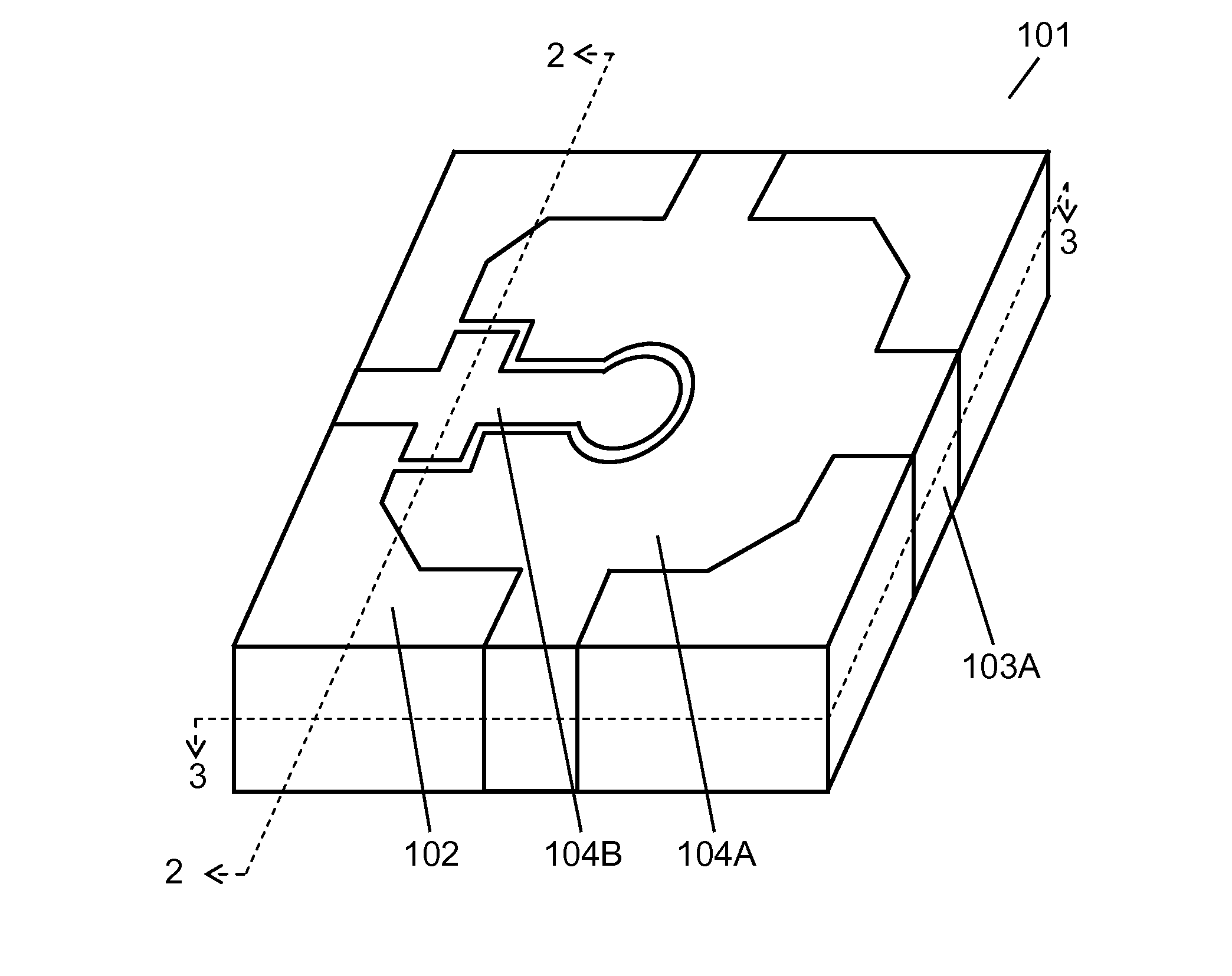
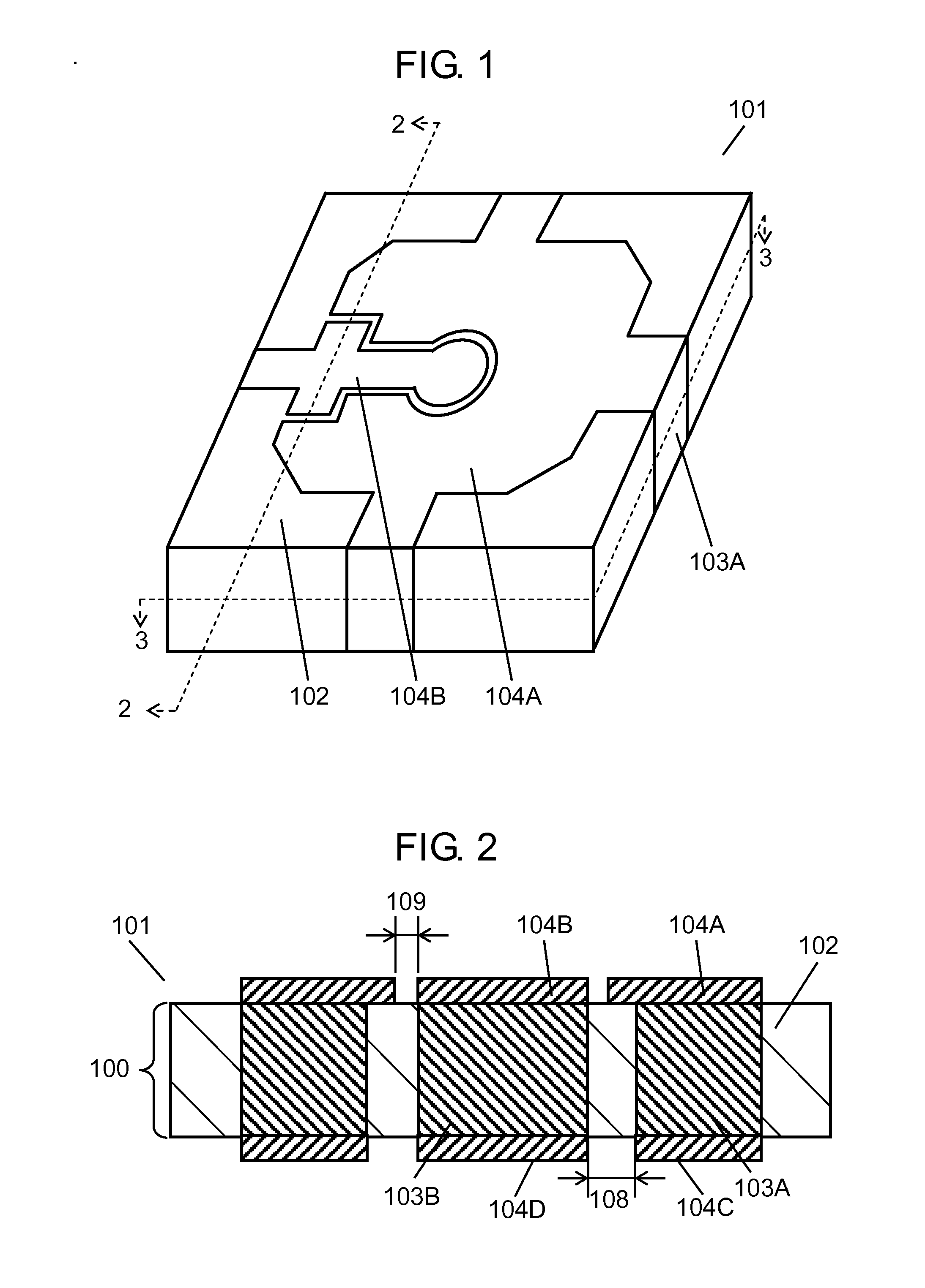
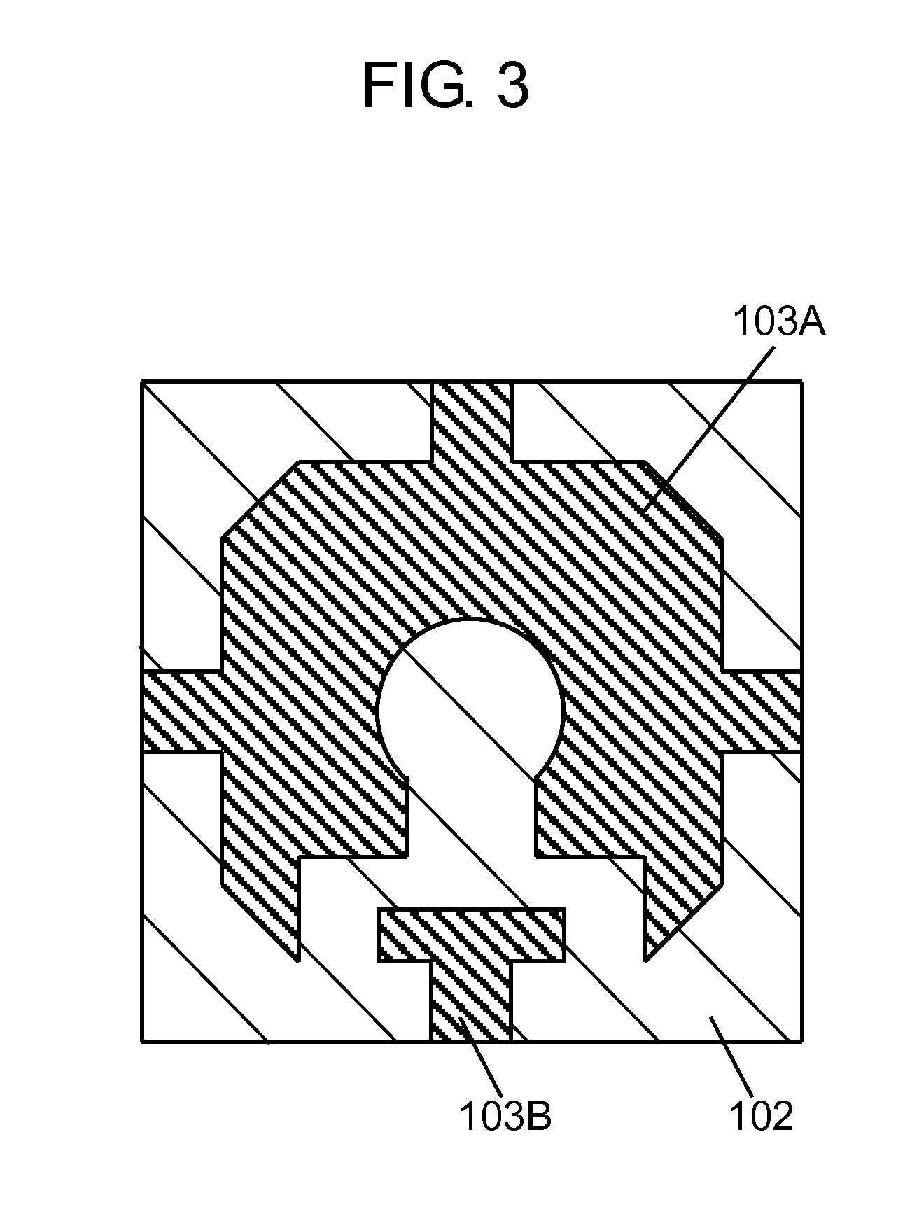
[0135]The following is a description of the analysis of the volume proportion of plate wirings 103A and 103B in base 100. More specifically, five wiring boards are manufactured corresponding to five different wiring boards 101 having different volume proportions of plate wirings 103A and 103B in base 100, namely, 10 vol %, 20 vol %, 40 vol %, 60 vol %, and 80 vol %. The measurement results include thermal resistance, elastic modulus, and bonding strength when light emitting element 111 is mounted on each of these wiring boards. Note that the present invention is not limited to the following example.

[0136]Regarding each of these five wiring boards, a square assembly of wiring boards of 50 mm is formed, and a 3.5 mm square wiring board is evaluated. Plate wirings 103A and 103B are made of a 0.3 mm thick copper alloy, and have a minimum wiring gap of 0.3 mm. FIGS. 16A to 16E show plan views of plate wirings 403 to 443, which are shown as schematic patterns of plate wirings 103A ...


PUM


Abstract

A wiring board includes a base in which plate wirings formed of a metal plate are integrally formed with an insulating portion made of resin or a resin composition and surface wirings electrically connected to the plate wirings. The base has first and second surfaces on which the surface wirings are formed. The surface wirings are thinner than the plate wirings, and the minimum wiring gap between the surface wirings is smaller than the minimum wiring gap between the plate wirings. One of the plate wirings has substantially the same shape as that of a region where the first top-surface wiring on the first surface and the first bottom-surface wiring on the second surface overlap with each other in the normal direction of the first surface. The first top-surface wiring and the first bottom-surface wiring are connected to each other through the above-mentioned one of the plate wirings.

Description

BACKGROUND[0001]1. Technical Field[0002]The present technical field relates to a wiring board including plate wirings, an insulating portion integrally formed therewith, and surface wirings formed on the principal planes thereof. The technical field also relates to a light emitting device including the wiring board and a light emitting element mounted thereon, and to methods for manufacturing the wiring board and the light emitting device.[0003]2. Background Art[0004]Light emitting elements such as light emitting diodes (hereinafter, LEDs) and semiconductor lasers are used in various light emitting devices. Among them, light emitting devices including LED bare chips are more compact and efficient than already available light sources with discharge or emission, and also have advantageous properties such as being resistant to vibration and repeated on-off operations. For these advantages, the use of light emitting devices has been expanding mainly in the illumination field.[0005]A lig...

Claims


Application Information

Patent Timeline
IPC IPC(8): H01L33/62H05K1/02
CPCH01L33/62H05K2201/09209H05K1/0296H01L23/49838H01L23/49861H01L23/49894H01L24/97H01L33/647H01L2224/16225H01L2924/07802H01L2924/12041H01L2924/00H01L2924/00011H01L2924/12035H01L2924/12042H01L2924/15787H05K1/0204H05K2201/10106H01L2924/01005
Inventor ASAHI, TOSHIYUKITANI, NAOYUKIKITAGAWA, YOSHITOOKAZAKI, YUTA
Owner PANASONIC INTELLECTUAL PROPERTY MANAGEMENT CO LTD
Why Eureka
Try Eureka