Systems and methods for testing and packaging a superconducting chip

a superconducting integrated circuit and packaging technology, applied in the field of superconducting integrated circuit testing and packaging, can solve the problems of contaminating the semiconductor facility, gold can contaminate the fabrication tool, and the superconducting integrated circuit containing gold is typically not processed by tools, so as to achieve convenient, fast and advantageous attachment and removal.

Active Publication Date: 2014-09-04
D WAVE SYSTEMS INC
View PDF5 Cites 62 Cited by
  • Summary
  • Abstract
  • Description
  • Claims
  • Application Information

AI Technical Summary

Problems solved by technology

This may be due to the fact that some of the materials used in superconducting integrated circuits can contaminate the semiconductor facilities.
For instance, gold may be used as a resistor in superconducting circuits, but gold can contaminate a fabrication tool used to produce CMOS wafers in a semiconductor facility.
Consequently, superconducting integrated circuits containing gold are typically not processed by tools which also process CMOS wafers.
Due to issues associated with superconducting circuits, not all semiconductor processes and techniques are necessarily transferrable to superconductor chip production.
Such changes and adjustments typically are not obvious and may require a great deal of experimentation.
The semiconductor industry faces problems and issues not necessarily related to the superconducting industry.
Likewise, problems and issues that concern the superconducting industry are often of little or no concern in standard semiconductor fabrication.
Two important challenges in the superconductor industry are: establishing continuous, uninterrupted superconductive electrical connections through solder bumps and providing solder bumps of uniform height to prevent the formation of opens or shorts.
However, neither gold nor copper are superconducting metals.
Non-superconducting materials such as gold and copper are undesirable in superconducting chip bonding as such materials will exhibit resistivity at cryogenic temperatures which produces heat that may hinder effective signal transmission and / or circuit performance.
Furthermore, non-superconducting metals such as gold or copper can interrupt a continuous superconducting current path due to their electrical resistance.
Wirings of copper lines are coated with a superconducting solder, such as an 80 / 20 mixture of Pb / Sn, and there are no pillars of UBM that provide structural support to the solder bumps which could result in non-uniform solder bump heights producing unintentional shorts, floating signals, and so forth.
Such a technique may be suited well for semiconductor fabrication, but cannot be used in the superconductor industry due to some of the materials used being non-superconducting.
There is also no mechanism for ensuring uniform solder bump height; thus, U.S. Pat. No. 5,440,239 does not teach superconductive electrical connections and does not teach uniform solder bump heights.
Clearly, these techniques for flip-chip bonding and interconnection and assembly of chips using transferable solder bumps are not ideal for testing and packaging a superconducting chip.

Method used


Image

  • Systems and methods for testing and packaging a superconducting chip
  • Systems and methods for testing and packaging a superconducting chip
  • Systems and methods for testing and packaging a superconducting chip

Examples


Embodiment Construction

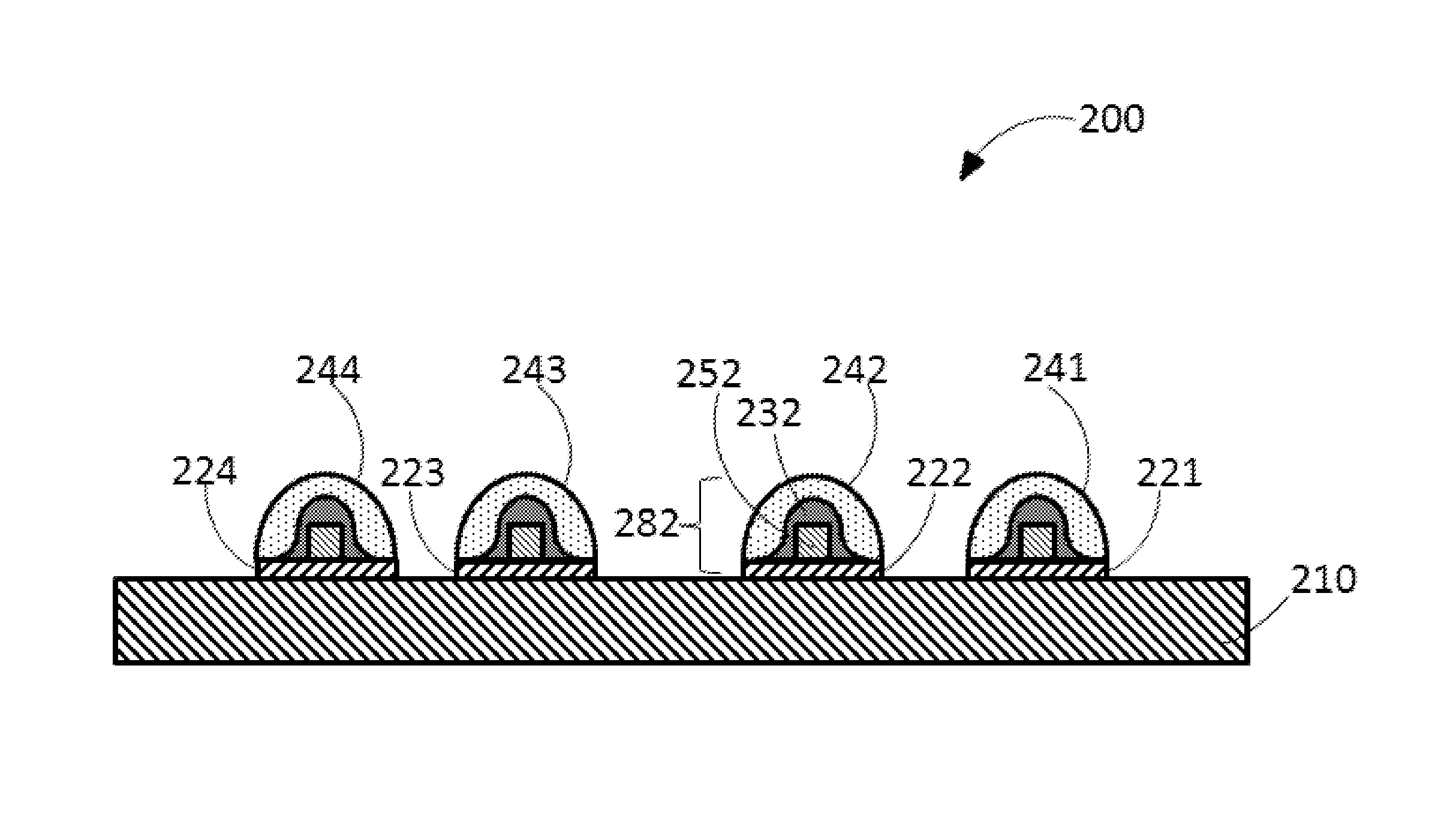
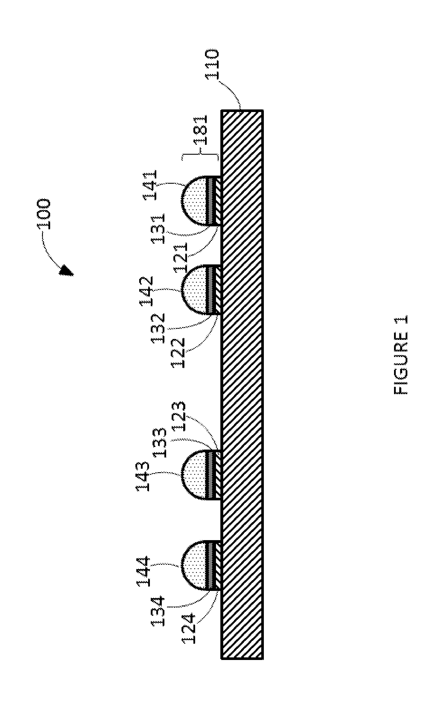
[0027]In the following description, some specific details are included to provide a thorough understanding of various disclosed embodiments. One skilled in the relevant art, however, will recognize that embodiments may be practiced without one or more of these specific details, or with other methods, components, materials, etc. In other instances, well-known structures associated with superconducting processors, such as superconducting devices (e.g., qubits), coupling devices, and control systems including microprocessors and drive circuitry have not been shown or described in detail to avoid unnecessarily obscuring descriptions of the embodiments of the present systems and methods.

[0028]Unless the context requires otherwise, throughout the specification and claims which follow, the word “comprise” and variations thereof, such as, “comprises” and “comprising” are to be construed in an open, inclusive sense, that is as “including, but not limited to.”

[0029]Reference throughout this s...


PUM


Abstract

Superconductive interconnection structures providing continuous, uninterrupted superconducting signal paths between a superconducting chip and a superconducting chip carrier are described. The superconductive interconnection structures employ superconducting solder bumps and pillars of Under Bump Metal (“UBM”). The superconductive interconnection structures are employed in a two-stage solder bumping process in which the superconducting chip is first bonded to a testing module for screening and then bonded to a chip packaging module for operation. Either the testing module or the chip packaging module, or both, may include a multi-chip module for carrying multiple superconducting chips simultaneously.

Description

BACKGROUND[0001]1. Field[0002]This disclosure generally relates to superconducting integrated circuits and particularly relates to testing and packaging superconducting integrated circuit chips.[0003]2. Superconducting Processor[0004]A superconducting integrated circuit may take the form of a superconducting processor, where the superconducting processor may be a classical processor or a quantum processor. A superconducting quantum processor may make use of quantum effects such as quantum tunneling, superposition, and / or entanglement whereas a superconducting classical processor may not make use of these effects, but may rather operate by emphasizing different principles, such as for example the principles that govern the operation of semiconducting classical processors. However, there may still be certain advantages to the implementation of such superconducting “classical” processors. Due to their natural physical properties, superconducting classical processors may be capable of h...

Claims


Application Information

Patent Timeline
Patent Type & Authority Applications(United States)
IPC IPC(8): H01L21/66H01L39/02H01L27/18H01L39/24
CPCH01L22/32H01L39/24H01L27/18H01L22/14H01L39/02G01R31/2891G01R31/2884H01L2224/13183H01L2224/13163H01L24/05H01L24/13H01L24/81H01L2224/05008H01L2224/05179H01L2224/05548H01L2224/05573H01L2224/05611H01L2224/13007H01L2224/13111H01L2224/13116H01L2224/13144H01L2224/13147H01L2224/13176H01L2224/13562H01L2224/1357H01L2224/13582H01L2224/136H01L2224/13611H01L2224/81191H01L2224/81192H01L2224/81815H01L2224/97H01L2224/05568H01L2224/05023H01L2224/16238H01L2924/35121H01L2924/15787H01L2224/0401H10N69/00H10N60/815H01L2924/00014H01L2924/014H01L2924/01076H01L2224/81H01L2924/00H10N60/01
Inventor BUNYK, PAUL I.
Owner D WAVE SYSTEMS INC
Why Eureka
Try Eureka