
Methods of Plasma Surface Treatment in a PVD Chamber

a plasma surface treatment and pvd technology, applied in the direction of vacuum evaporation coating, sequential/parallax process reactions, coatings, etc., can solve the problems of limited specific process performance and lack of flexibility, and achieve the effect of reducing or eliminating any plasma formation within the gap

Inactive Publication Date: 2014-09-18
INTERMOLECULAR
View PDF6 Cites 3 Cited by
  • Summary
  • Abstract
  • Description
  • Claims
  • Application Information

AI Technical Summary

Benefits of technology

The patent describes a device called a biasable pedestal that can be used in a physical vapor deposition chamber for surface treatment. This device allows for both sputter deposition and plasma treatment in the same chamber, eliminating the need for a separate plasma chamber. Additionally, the patent describes a method for combining these surface treatments by shielding the substrate surface while exposing at least one isolated region, which reduces or eliminates plasma formation within a small dark space gap. Overall, this patent provides a technical solution for improving the efficiency and precision of surface treatment processes.

Problems solved by technology

While PVD tools are commonly used in the industry, they are limited to performing specific processes and do not permit much flexibility.

Method used


Image

  • Methods of Plasma Surface Treatment  in a PVD Chamber
  • Methods of Plasma Surface Treatment  in a PVD Chamber
  • Methods of Plasma Surface Treatment  in a PVD Chamber

Examples


Embodiment Construction

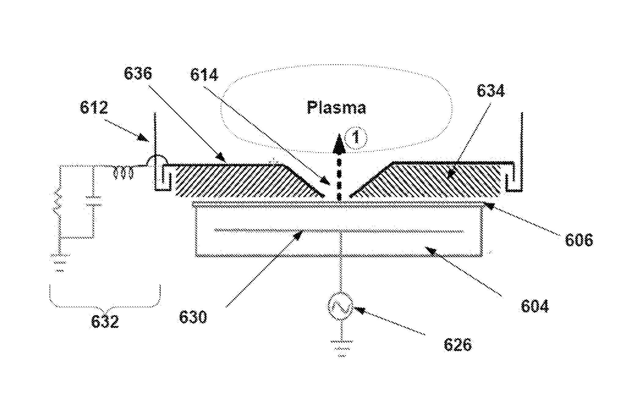
[0025]Some embodiments of the invention are directed to combined sputter deposition and plasma processes being performed in one process chamber. The chamber may include multiple sputter guns. An aperture and a grounded shield are placed above the substrate. The bottom of the aperture is flush with the bottom of the lower shield so that a small, constant dark-space gap is formed between the substrate and the aperture. A dielectric material may be used in the dark-space gap. The substrate is supported by a substrate support, such as an electrostatic chuck. A bias voltage can be applied to the substrate support, and plasma may be ignited with the one or more sputter guns while performing plasma processes (e.g. plasma etch or plasma surface treatment) in the chamber. The chamber is capable of performing both PVD sputter deposition and plasma processes, eliminating the need for a separate plasma chamber.

[0026]As used herein, the phrases “plasma processes” and “plasma processing” will be ...


PUM

PropertyMeasurementUnit
Electric potential / voltageaaaaaaaaaa

Abstract

Combinatorial processing of a substrate comprising site-isolated sputter deposition and site-isolated plasma processing can be performed in a same process chamber. The process chamber, configured to perform sputter deposition and plasma processing, comprises a grounded shield having at least an aperture disposed above the substrate to form a small, dark space gap to reduce or eliminate any plasma formation within the gap. The plasma processing may include plasma etching or plasma surface treatment.

Description

TECHNICAL FIELD[0001]The present disclosure relates generally to semiconductor manufacturing and in particular to radio frequency (RF) plasma treatment in a plasma deposition chamber with a biasable pedestal for full wafer and combinatorial processing.BACKGROUND[0002]Plasma processing or manufacturing techniques are used in the manufacture of integrated circuits (IC) semiconductor devices, flat panel displays, optoelectronics devices, data storage devices, magneto electronic devices, magneto optic devices, packaged devices, and the like.[0003]Deposition processes are commonly used in semiconductor manufacturing to deposit a layer of material onto a substrate. Physical vapor deposition (PVD) is one example of a deposition process, and sputter deposition or sputtering is a common physical vapor deposition method. In sputtering, ions or neutral species are ejected from a target material by high-energy particle bombardment and then deposited onto the substrate using plasma. In some proc...

Claims


Application Information

Patent Timeline
IPC IPC(8): C23C14/35
CPCC23C14/35B01J19/0046C23C14/042C23C14/345B01J2219/0043B01J2219/00443B01J2219/00527B01J2219/00635B01J2219/0075B01J2219/00756
Inventor BODKE, ASHISHKARLSSON, OLOVKASHEFI, KEVINLANG, CHI-IPRAMANIK, DIPANKARYANG, HONG SHENGZHANG, XUENA
Owner INTERMOLECULAR
Learn More