

Silane and borane treatments for titanium carbide films
- Summary
- Abstract
- Description
- Claims
- Application Information
AI Technical Summary
Benefits of technology
Problems solved by technology
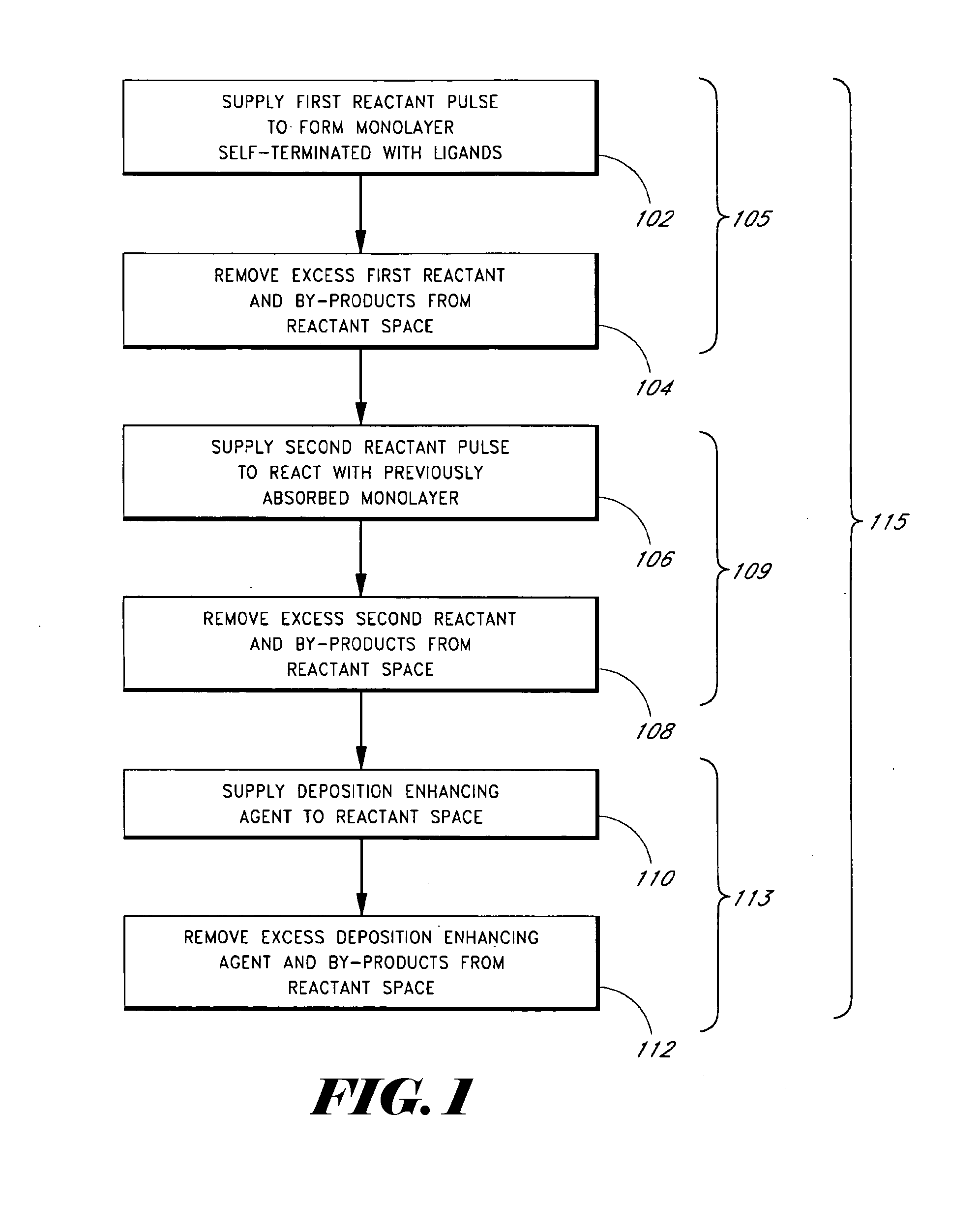
Method used
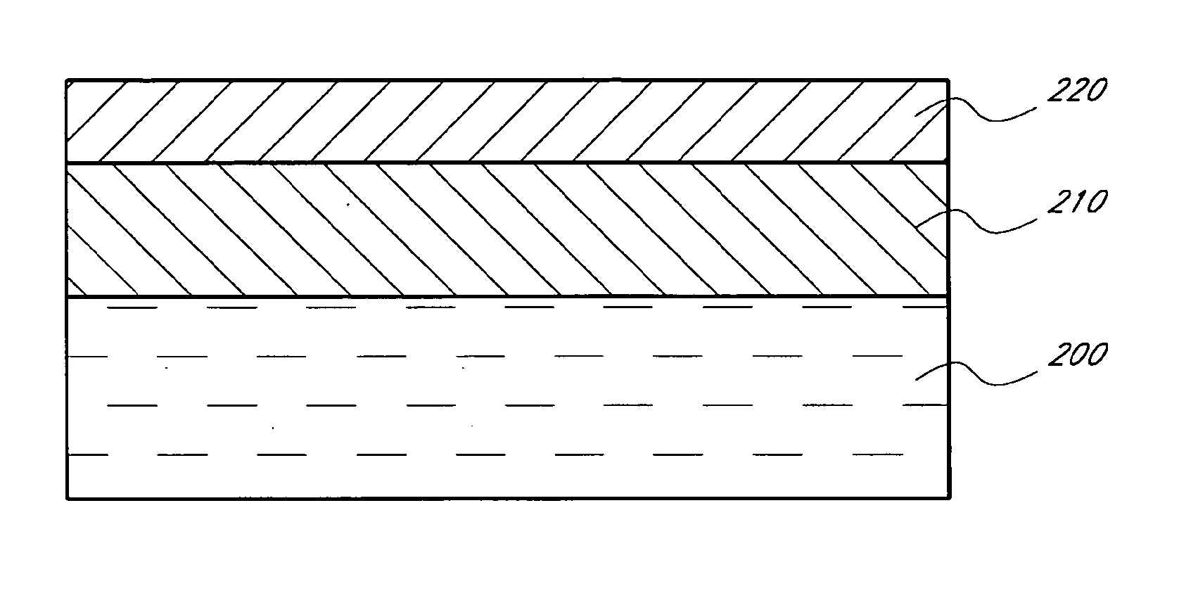
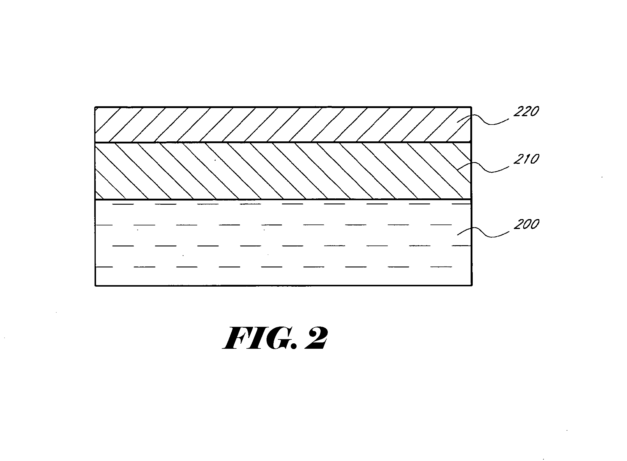
Image

Examples
example 1
TiC Films
[0112]Using the methods disclosed here in, various titanium carbide thin films were deposited. The thin film was then analyzed using Rutherford backscattering spectrometry, or RBS, to determine the composition of the various films.
[0113]After analyzing the various films, it was determined that they the following ranges of compositions on an atomic basis: about 17-20% Ti, about 17-27% Al, about 16-42% Si, and about 21-39% C.
example 2
TiAlC and TiAlSiC in a single wafer reactor
[0114]Titanium-aluminium carbide (TiAlC) and titanium-aluminum-carbide-silicon (TiAlSiC) thin films were deposited by Atomic layer deposition (ALD) in Pulsar® 2000 R&D reactor using TiCl4 as the titanium source and Al(CH2CH3)3 as the aluminum and carbon source for the TiAlC films and in addition disilane (Si2H6) or trisilane (Si3H8) was used as a silicon source for TiAlSiC films.
[0115]TiAlC and TiAlSiC films were deposited using alternate and sequential pulses of TiCl4 and Al(CH2CH3)3 and in the case of TiAlSiC films additional alternate and sequential pulses of disilane (Si2H6) or trisilane (Si3H8) were provided. TiAlC films were also soaked with disilane (Si2H6) or trisilane (Si3H8) for about 1 minute. Films were deposited and treated at a reaction temperature of about 415° C. TiCl4 was pulsed for 0.05 s and purged for 5 s. Al(CH2CH3)3 was pulsed for 0.5 s and purged for 5 s. Si2H6 or Si3H8 was pulsed for 0.5 s and purged for 5 s. The Al(...
PUM
 Abstract
Description
Claims
Application Information