Semiconductor device

Active Publication Date: 2014-09-25
SEMICON ENERGY LAB CO LTD
View PDF2 Cites 132 Cited by
  • Summary
  • Abstract
  • Description
  • Claims
  • Application Information

AI Technical Summary

Benefits of technology

[0017]According to one embodiment of the present invention, a nonvolatile semiconductor device which can be driven at low voltage can be provided. According to one embodiment of the present invention, a nonvolatile semiconductor

Problems solved by technology

The SRAM achieves high-speed operation with miniaturization of a transistor; however, there is a problem in that as the transistor is miniaturized, an increase in leakage current becomes obvious and thus, power consumption is increased.
However, a flip-flop used as a register and an SRAM

Method used


Image

  • Semiconductor device
  • Semiconductor device
  • Semiconductor device

Examples


embodiment 1

[0036]In this embodiment, an example of a semiconductor device including a nonvolatile portion and a volatile portion is described.

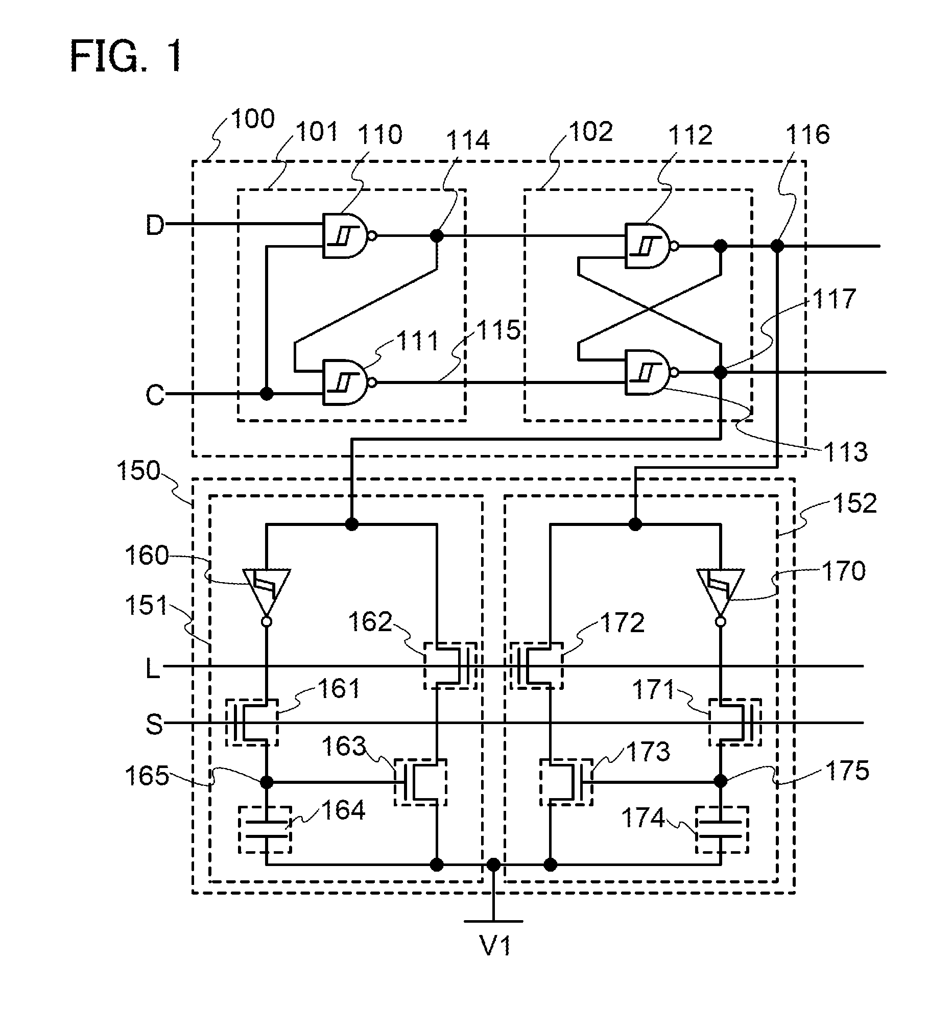
[0037]FIG. 1 is a circuit diagram of a latch circuit. The latch circuit illustrated in FIG. 1 includes a first memory circuit portion 100 and a second memory circuit portion 150. The first memory circuit portion 100 has a function of holding a potential corresponding to data in a period when power supply voltage is continuously supplied. The second memory circuit portion 150 has a function of holding a potential corresponding to data in a period when the supply of power supply voltage is stopped.

[0038]The first memory circuit portion 100 includes a gate portion 101 and a latch portion 102.

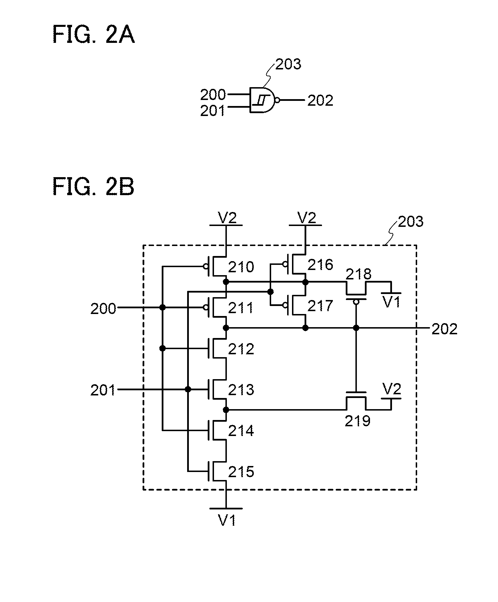
[0039]The gate portion 101 includes a Schmitt trigger NAND circuit (hereinafter also referred to as ST-NAND) 110 and an ST-NAND 111.

[0040]A first input terminal of the ST-NAND 110 is electrically connected to a wiring to which a data signal D is supplied. A second input...

embodiment 2

[0105]In this embodiment, an example of a semiconductor device including a nonvolatile portion and a volatile portion is described.

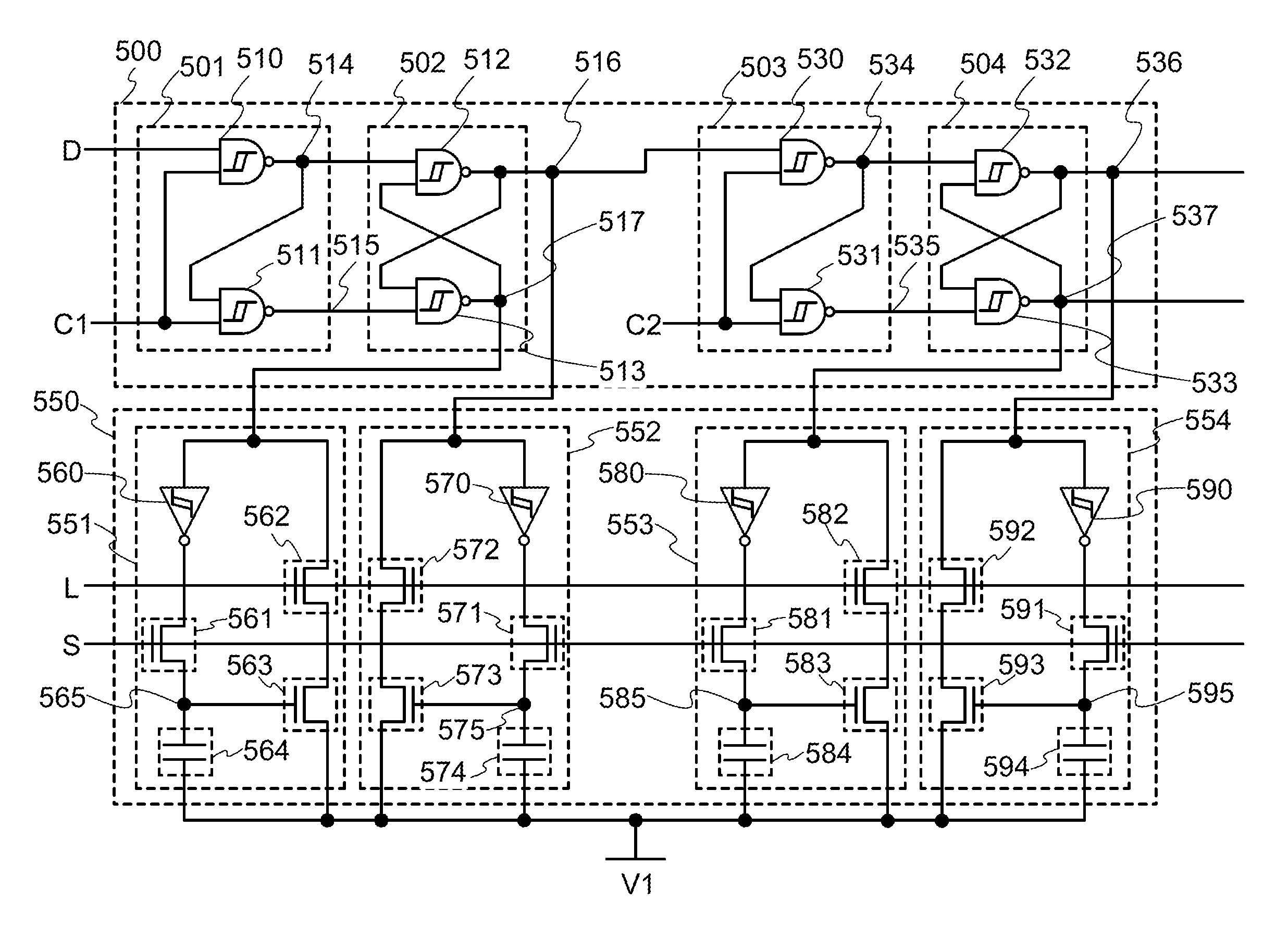
[0106]FIG. 5 is a circuit diagram of a flip-flop circuit. The flip-flop circuit illustrated in FIG. 5 includes a first memory circuit portion 500 and a second memory circuit portion 550. The first memory circuit portion 500 has a function of holding a potential corresponding to data in a period when power supply voltage is continuously supplied. The second memory circuit portion 550 has a function of holding a potential corresponding to data in a period when the supply of power supply voltage is stopped.

[0107]The first memory circuit portion 500 includes a gate portion 501, a master latch 502, a gate portion 503, and a slave latch 504.

[0108]The gate portion 501 includes an ST-NAND 510 and an ST-NAND 511.

[0109]A first input terminal of the ST-NAND 510 is electrically connected to a wiring to which a data signal D is supplied. A second input terminal of th...

embodiment 3

[0164]In this embodiment, an example of a semiconductor device including a nonvolatile portion and a volatile portion is described.

[0165]FIG. 7 is a circuit diagram of a flip-flop circuit. The flip-flop circuit illustrated in FIG. 7 has a configuration different from that of the flip-flop circuit illustrated in FIG. 5. The flip-flop circuit illustrated in FIG. 7 includes a first memory circuit portion 400 and a second memory circuit portion 450. The first memory circuit portion 400 has a function of holding a potential corresponding to data in a period when power supply voltage is continuously supplied. The second memory circuit portion 450 has a function of holding a potential corresponding to data in a period when the supply of power supply voltage is stopped.

[0166]The first memory circuit portion 400 includes a gate portion 401 and a latch portion 402.

[0167]The gate portion 401 includes an ST-NAND 410, an ST-NAND 411, an ST-NAND 412, a Schmitt trigger AND circuit (hereinafter als...


PUM


Abstract

A nonvolatile semiconductor device which can be driven at low voltage is provided. A nonvolatile semiconductor device with low power consumption is provided. A Schmitt trigger NAND circuit and a Schmitt trigger inverter are included. Data is held in a period when the supply of power supply voltage is continued, and a potential corresponding to the data is stored at a node electrically connected to a capacitor before a period when the supply of power supply voltage is stopped. By utilizing a change in channel resistance of a transistor whose gate is connected to the node, the data is restored in response to the restart of the supply of power supply voltage.

Description

TECHNICAL FIELD[0001]The present invention relates to a semiconductor device. The present invention particularly relates to a semiconductor device in which the supply of power supply voltage is stopped as appropriate.[0002]Note that in this specification, a semiconductor device means a device including a semiconductor element or a circuit including a semiconductor element.BACKGROUND ART[0003]A semiconductor device such as a programmable logic device (PLD) or a central processing unit (CPU) has a variety of configurations depending on its application. The semiconductor device generally includes a memory device; the PLD includes a register and a configuration memory, and the CPU includes a register and a cache memory.[0004]These memory devices need to operate at higher speed in writing and reading data than a main memory for which a DRAM is generally used. Thus, in many cases, a flip-flop is used as a register, and a static random access memory (SRAM) is used as a configuration memory...

Claims


Application Information

Patent Timeline
IPC IPC(8): G11C5/06
CPCG11C5/06G11C11/24G11C14/0054G11C7/1057G11C7/1051
Inventor AOKI, TAKESHIKUROKAWA, YOSHIYUKIKOZUMA, MUNEHIRO
Owner SEMICON ENERGY LAB CO LTD
Why Eureka
Try Eureka