Organic el element

a technology of organic elements and elements, applied in the field of organic elements, can solve the problems that the light generated at the organic layer cannot be extracted to the outside sufficiently, and the external extraction efficiency cannot be achieved, so as to achieve the effect of light emission efficiency, improved light extraction efficiency, and higher level

Inactive Publication Date: 2014-10-16
JX NIPPON OIL & ENERGY CORP
View PDF2 Cites 50 Cited by
  • Summary
  • Abstract
  • Description
  • Claims
  • Application Information

AI Technical Summary

Benefits of technology

[0034]According to the present invention, it is possible to provide an organic EL element which can achieve improvement in the light extraction efficiency thereof at a higher level and can achieve a light emission efficiency at a sufficiently high level.

Problems solved by technology

However, such an organic EL element has a problem that light generated at the organic layer cannot be extracted to the outside sufficiently.
Specifically, there is a problem that a large proportion of light generated at the organic layer disappears as heat during repetition of multiple reflections inside the element, or propagates inside the element and exits from end portions of the element, so that a sufficient external extraction efficiency cannot be achieved.

Method used


Image

  • Organic el element
  • Organic el element
  • Organic el element

Examples


example 1

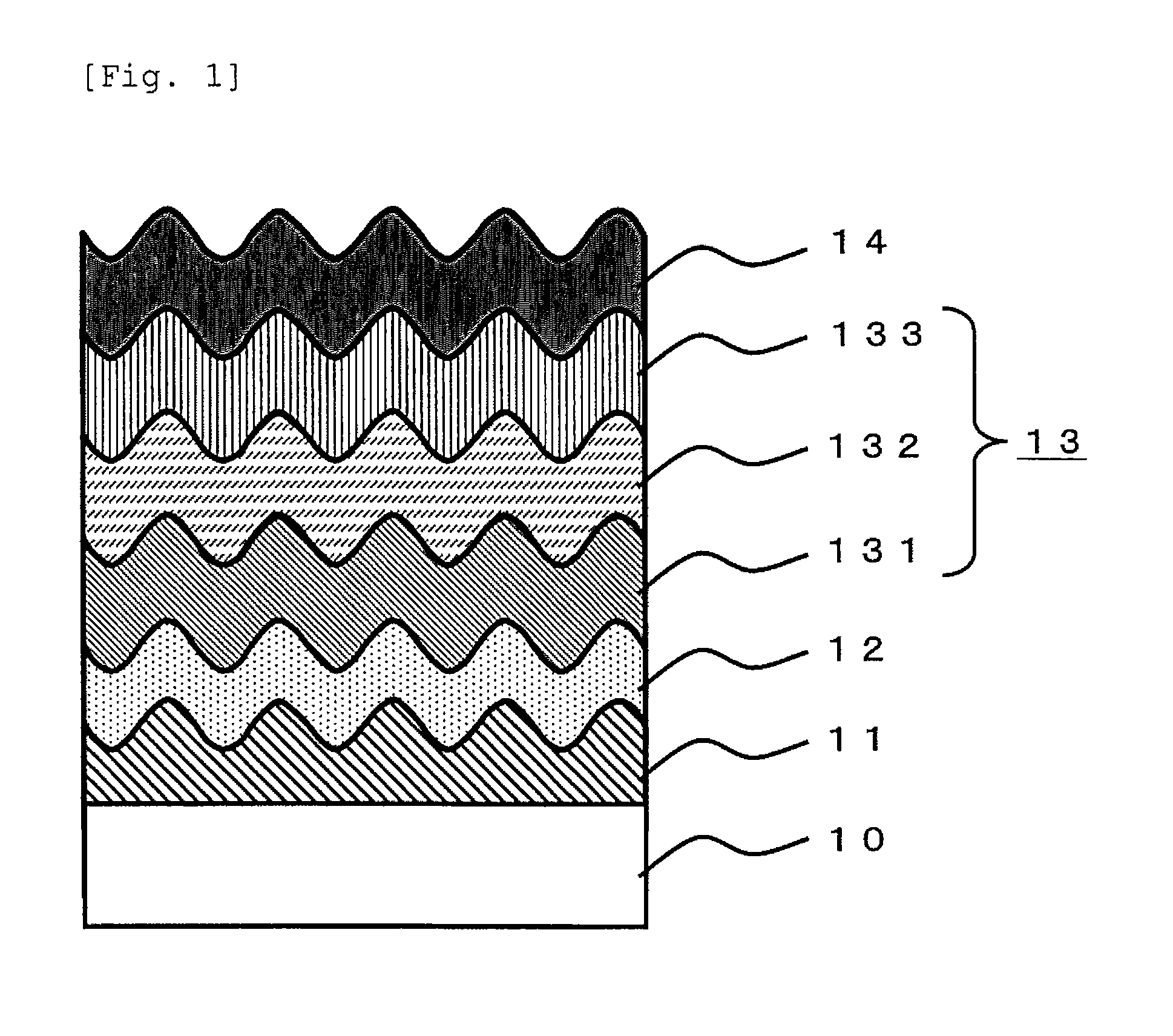
[0270]An organic EL element having the structure shown in FIG. 11 (the structure of transparent supporting substrate 10 / diffraction grating 11 / transparent electrode 12 / hole transporting layer 131 / light emitting layer 132 / hole blocking layer 134 / electron transporting layer 133 / cathode buffer layer 16 / metal electrode 14 stacked in this order) was manufactured as follows.

[0271]

[0272]First, a b lock copolymer (A) used in a step of preparing a master block (mold) is described.

[0273][Block Copolymer (A)]

[0274]A block copolymer of PS and PMMA (manufactured by Polymer Source Inc,),

[0275]Mn of PS segment=868,000,

[0276]Mn of PMMA segment=857,000,

[0277]Mn of block copolymer=1,725,000,

[0278]Volume ratio of PS segment to PMMA segment (PS:PMMA)=53:47,

[0279]Molecular weight distribution (Mw / Mn)=1.30,

[0280]Tg of PS segment=96° C.,

[0281]Tg of PMMA segment=110° C.

[0282]As the block copolymer (A), a block copolymer being manufactured by Polymer Source Inc, and containing polystyrene (hereinafter, abbr...

example 2

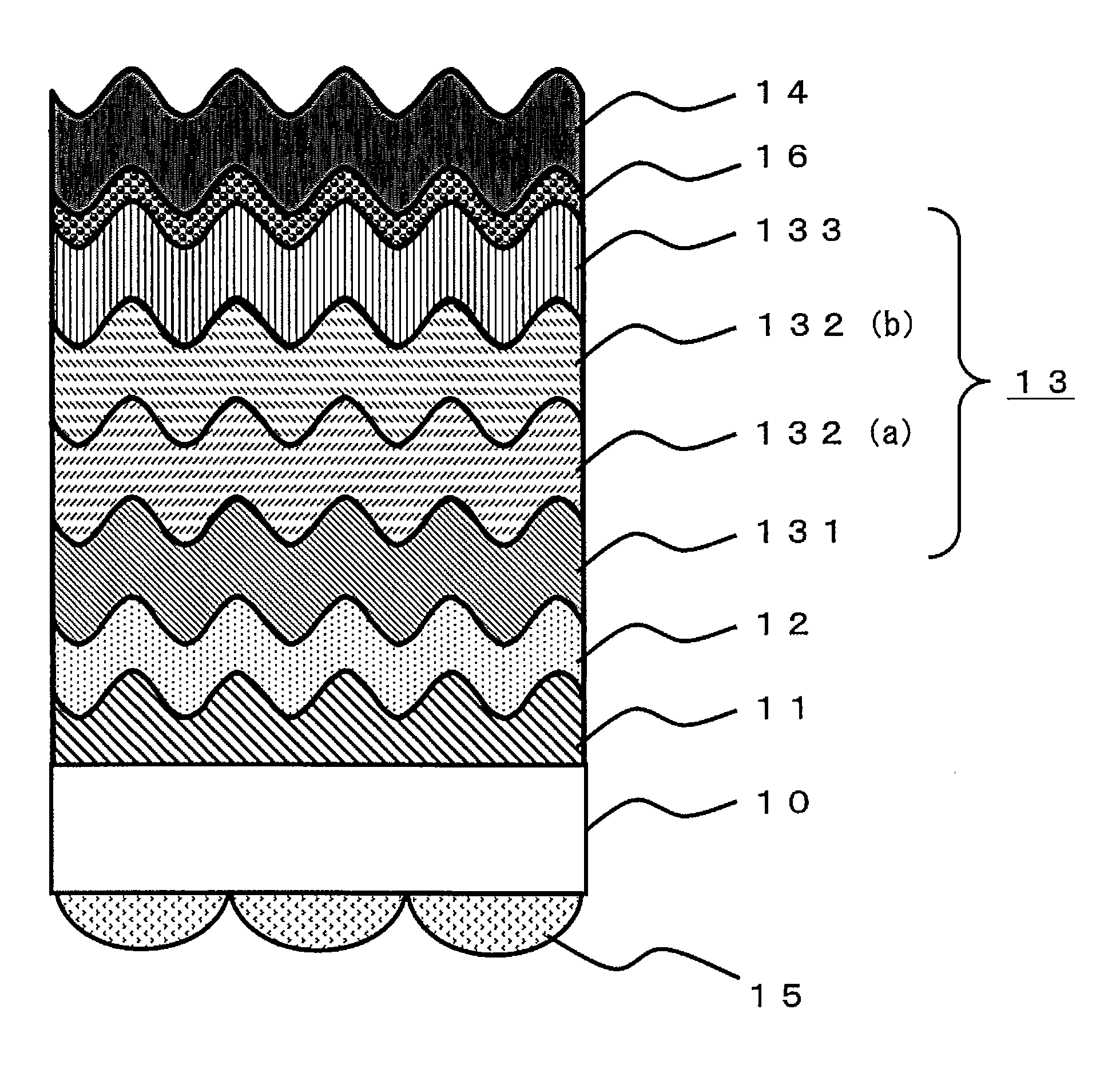
[0319]A diffraction grating (concavity and convexity layer) was manufactured on a glass substrate by employing the same method as in the diffraction grating formation step employed in Example 1. After the diffraction grating was formed on the glass substrate, an organic EL element having a structure as shown in FIG. 13 (the structure of transparent supporting substrate 10 / diffraction grating 11 / transparent electrode 12 / hole transporting layer 131 / first light emitting layer 132 (a) / second light emitting layer 132 (b) / electron transporting layer 133 / cathode buffer layer 16 / metal electrode 14 stacked in this order) was manufactured in the same manner as in Example 1, except that an organic EL element formation step 2 described later was conducted instead of the organic EL element formation step 1.

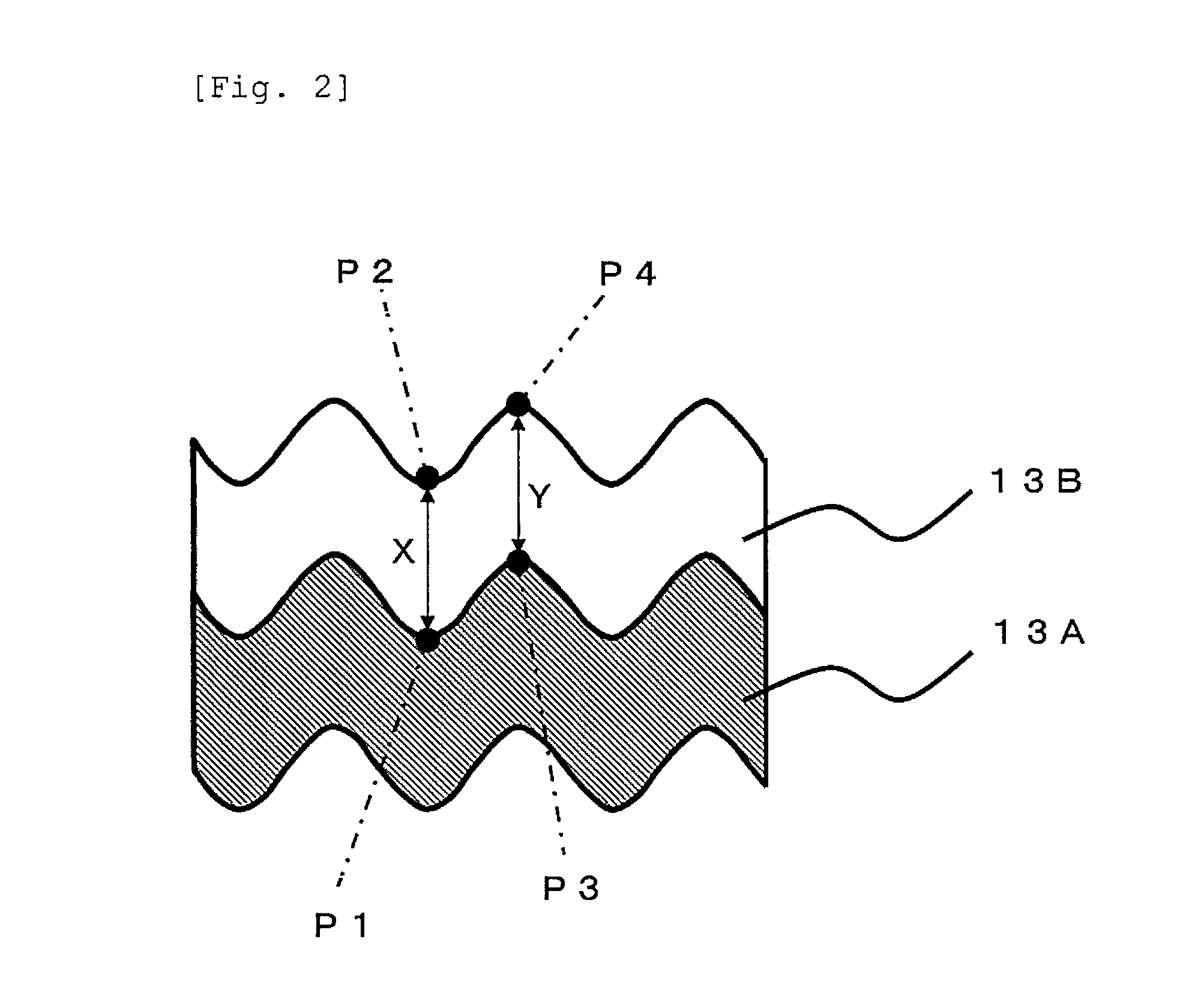
[0320]In addition, as in the case of Example 1, it was found that a Fourier-transformed image of the diffraction grating obtained in Example 2 showed a circular pattern substantially centered ...

example 3

[0329]A diffraction grating (concavity and convexity layer) was manufactured on a glass substrate by employing the same method as in the diffraction grating formation step employed in Example 1. Subsequently, an organic EL element having a structure of transparent supporting substrate (glass substrate) / diffraction grating / transparent electrode (ITO) / hole transporting layer (TCTA) / light emitting layer (TCTA:7.0% by mass of Ir(ppy)3) / electron transporting layer (TpBi) / cathode buffer layer made of metal-based material (LiF) / metal electrode (Al) stacked in this order was manufactured in the same manner as in Example 1, except that an organic EL element formation step 3 described later was conducted instead of the organic EL element formation step 1.

[0330]In addition, regarding a Fourier-transformed image of the diffraction grating obtained in Example 3, it was found, as in the case of Example 1, that the Fourier-transformed image showed a circular pattern substantially centered at an or...


PUM


Abstract

An organic EL element including: a transparent supporting substrate; a diffraction grating having a concavity and convexity layer with first concavities and convexities formed on a surface thereof and disposed on the transparent supporting substrate; and a transparent electrode, an organic layer, and a metal electrode which are stacked in this order on the diffraction grating and formed into such shapes that a shape of the first concavities and convexities formed on the surface of the diffraction grating is maintained, the organic layer comprising at least a light emitting layer. The organic EL element satisfies specified conditions (A) to (C).

Description

TECHNICAL FIELD[0001]The present invention relates to an organic EL element.BACKGROUND ART[0002]Organic electroluminescence elements (organic EL elements) have been used as self-luminous elements for image display devices, such as displays, and for surface light sources. Such an organic EL element (organic light-emitting diode (OLED)) is generally prepared by stacking a transparent electrode serving as an anode, an organic layer, and a metal electrode serving as a cathode in this order on a transparent supporting substrate such as a glass substrate or a transparent plastic film. Thus, upon application of a voltage between the transparent electrode and the metal electrode, electrons supplied from the cathode and holes supplied from the anode are recombined at the organic layer. Then, when excitons generated by the recombination undergo transition from an excited state to a ground state, EL emission occurs. Light of the EL emission goes through the transparent electrode, and then is e...

Claims


Application Information

Patent Timeline
Patent Type & Authority Applications(United States)
IPC IPC(8): H01L51/52H01L51/50
CPCH01L51/5275G02B5/1866H01L51/5072H01L51/5056H01L51/5016H10K50/858G02B5/1814G02B5/1852H10K50/11H10K50/15H10K50/16H10K2101/10
Inventor SATO, YUSUKENISHIMURA, SUZUSHIJEONG, SOON MOON
Owner JX NIPPON OIL & ENERGY CORP
Why Eureka
Try Eureka