Semiconductor device and method of manufacturing the same

a technology of semiconductors and semiconductors, applied in the direction of semiconductor devices, electrical equipment, basic electric elements, etc., can solve the problems of affecting the reliability of the apparatus, etc., and achieve the effect of reducing failure, improving apparatus characteristics and reliability

Active Publication Date: 2014-10-16
SUMITOMO ELECTRIC DEVICE INNOVATIONS
View PDF4 Cites 1 Cited by
  • Summary
  • Abstract
  • Description
  • Claims
  • Application Information

AI Technical Summary

Benefits of technology

[0016]According to the invention, in the semiconductor device using the nitride semiconductor, it is possible to suppress failure due to a high electric field generated on the ohmic electrodes and to improve apparatus characteristics and reliability.

Problems solved by technology

In this case, reliability of the apparatus may be decreased by electrical conduction destruction, and the characteristics of the apparatus may be changed by current collapse.

Method used


Image

  • Semiconductor device and method of manufacturing the same
  • Semiconductor device and method of manufacturing the same
  • Semiconductor device and method of manufacturing the same

Examples


example 1

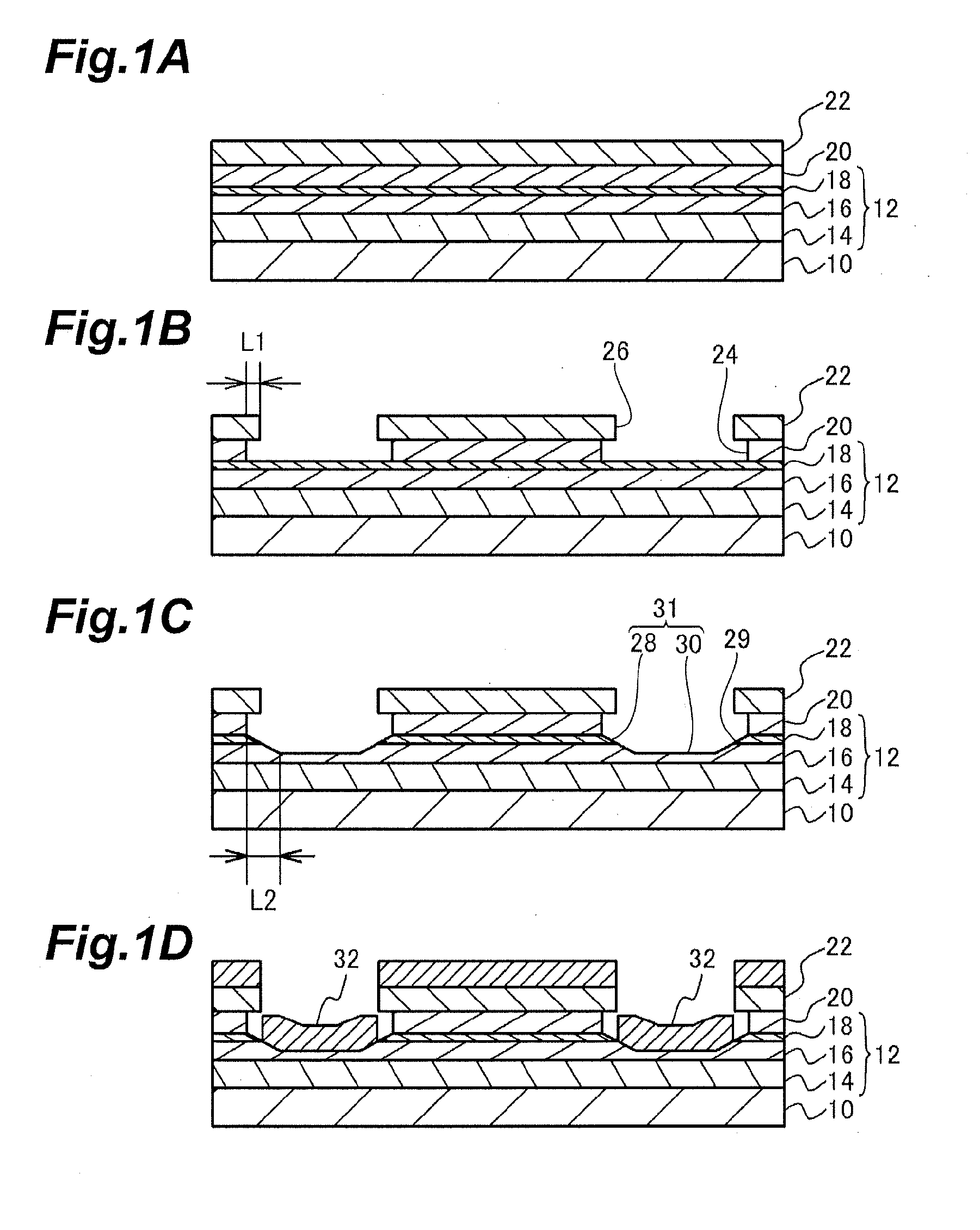
[0024]FIGS. 1A to 2D are diagrams showing a process for manufacturing a semiconductor device according to Example 1 of an aspect of this invention. As shown in FIG. 1A, a nitride semiconductor layer 12 is formed on a substrate 10 using a MOCVD (Metal Organic Chemical Vapor Deposition) method. As the substrate 10, for example, a SiC substrate having a (0001) principal surface can be used. The nitride semiconductor layer 12 is formed by laminating a first nitride semiconductor layer 14, a second nitride semiconductor layer 16, and a third nitride semiconductor layer 18 in this order. The nitride semiconductor layer 12 may include a doping region containing dopant. For example, Si or the like can be used as the dopant.

[0025]The first nitride semiconductor layer 14 is a layer including an electron transit layer, and can be formed of, for example, non-doped gallium nitride (GaN) layer having a thickness of 1000 nm. The first nitride semiconductor layer 14 may include a buffer layer in ad...

example 2

[0043]Example 2 is an example where single-layer resist is used in a process for forming an opening in a second nitride semiconductor layer.

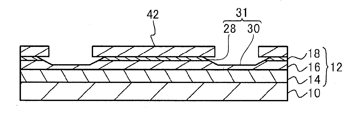
[0044]FIGS. 6A and 6B are diagrams showing a process for manufacturing a semiconductor device according to Example 2, and correspond to the etching process shown in FIGS. 1B and 1C. Other processes are the same as those in Example 1, thus description thereof will not be repeated.

[0045]First, as shown in FIG. 6A, resist 42 is formed on the third nitride semiconductor layer 18, and patterning is performed in conformity with the shapes of the ohmic electrodes (source electrode and drain electrode). Next, as shown in FIG. 6B, the third nitride semiconductor layer 18 and the second nitride semiconductor layer 16 are isotropically etched with the resist 42 as a mask. With this process, the opening 28 is formed in the third nitride semiconductor layer 18, the concave portion 30 is formed in the second nitride semiconductor layer 16, and the concave por...


PUM


Abstract

A semiconductor device includes a semiconductor layer formed on a substrate, an electrode contact window that includes a recess formed on a surface of the semiconductor layer, an inner wall having a slope, and a source electrode, a drain electrode, and a gate electrode formed on the semiconductor layer, in which the drain electrode is in contact with the slope of the inner wall.

Description

BACKGROUND OF THE INVENTION[0001]1. Field of the Invention[0002]The present invention relates to a semiconductor device using a nitride semiconductor and a method of manufacturing the same.[0003]2. Related Background Art[0004]A semiconductor device using a nitride semiconductor is used as a power device or the like which operates at high frequency and at high output power. In particular, as a semiconductor device suitable for amplification in a high-frequency band, such as a microwave, a quasi-millimeter wave, and a millimeter wave, for example, a field effect transistor (FET) of a high electron mobility transistor (HEMT) or the like is known.[0005]Japanese Unexamined Patent Application Publication No. 2012-23213 discloses a field effect transistor in which a part of a nitride semiconductor layer is removed (recessed) and a gate electrode and an ohmic electrode (source electrode and drain electrode) are formed on the nitride semiconductor layer.SUMMARY OF THE INVENTION[0006]In the c...

Claims


Application Information

Patent Timeline
Patent Type & Authority Applications(United States)
IPC IPC(8): H01L29/205H01L29/66H01L29/778
CPCH01L29/205H01L29/7786H01L29/66462
Inventor NISHI, MASAHIRO
Owner SUMITOMO ELECTRIC DEVICE INNOVATIONS
Why Eureka
Try Eureka