Method of manufacturing thin-film transistor, method of manufacturing organic light-emitting display device including the same, and thin-film transistor and organic light-emitting display device manufactured using the methods

Active Publication Date: 2014-10-23
SAMSUNG DISPLAY CO LTD
View PDF3 Cites 12 Cited by
  • Summary
  • Abstract
  • Description
  • Claims
  • Application Information

AI Technical Summary

Benefits of technology

[0021]A carrier density of the lower electrode of the

Problems solved by technology

When the active layer is formed of amorphous silicon, it is difficult to implement a driving circuit operating at a high speed since mobility of charges is low, and when the active layer is formed of poly-silicon, mobility is high, but an additional compensation circuit is necessary since a threshold voltage is not uniform, In addition, since a comparable method of manufacturing a thin-film transisto

Method used


Image

  • Method of manufacturing thin-film transistor, method of manufacturing organic light-emitting display device including the same, and thin-film transistor and organic light-emitting display device manufactured using the methods
  • Method of manufacturing thin-film transistor, method of manufacturing organic light-emitting display device including the same, and thin-film transistor and organic light-emitting display device manufactured using the methods
  • Method of manufacturing thin-film transistor, method of manufacturing organic light-emitting display device including the same, and thin-film transistor and organic light-emitting display device manufactured using the methods

Examples


Embodiment Construction

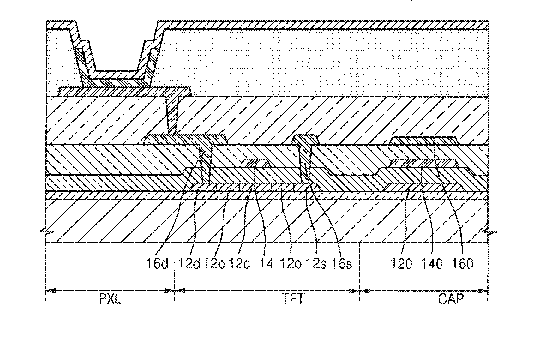
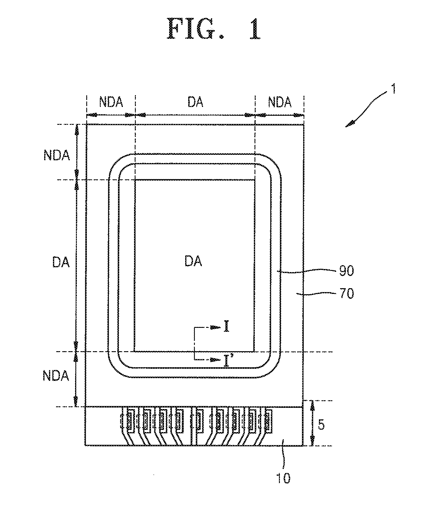
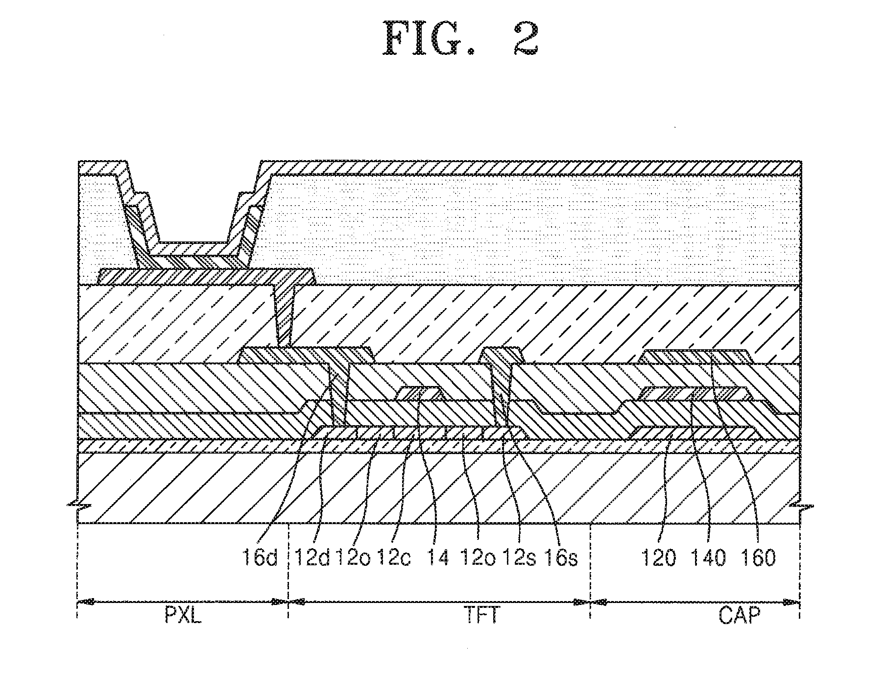
[0034]The detailed description of embodiments of the present invention to be described below refers to the accompanying drawings in which specific embodiments for carrying out the present invention are shown as illustrations. The embodiments are described in detail for one of ordinary skill in the art to sufficiently carry out the present invention. It should be understood that various embodiments of the present invention are different from each other but do not have to be exclusive from each other. For example, specific shapes, structures and characteristics set forth in the specification may be modified and implemented from one embodiment to another embodiment without departing from the spirit and scope of the present invention. In addition, it should be understood that a position or disposition of each component in each embodiment may also be changed without departing from the spirit and scope of the present invention. Therefore, the detailed description to be described below is ...


PUM


Abstract

A method of manufacturing a thin-film transistor includes: forming an oxide semiconductor pattern including a first region and a second region on a substrate; forming an insulation film on the substrate to cover the oxide semiconductor pattern; removing the insulation film on the second region through patterning; increasing carrier density of the first region of the oxide semiconductor pattern through an annealing process; forming a gate electrode on the insulation film so that the gate electrode is insulated from the oxide semiconductor pattern and overlaps the second region; and forming a source electrode and a drain electrode to be insulated from the gate electrode and contact the first region.

Description

CROSS-REFERENCE TO RELATED APPLICATION[0001]This application claims priority to and the benefit of Korean Patent Application No. 10-2013-0043032, filed on Apr. 18, 2013, in the Korean Intellectual Property Office, the entire content of which is incorporated herein by reference.BACKGROUND[0002]1. Field[0003]The following description relates to a method of manufacturing a thin-film transistor having an active layer that includes an oxide semiconductor, a method of manufacturing an organic light-emitting display device including the same, and a thin-film transistor and an organic light-emitting display device manufactured using the methods.[0004]2. Description of the Related Art[0005]A flat display device, such as an organic light-emitting display device, a liquid crystal display device, or the like, is manufactured on a substrate on which at least one thin-film transistor, at least one capacitor, and the like for driving the flat display device and a pattern including wirings for conn...

Claims


Application Information

Patent Timeline
IPC IPC(8): H01L29/786H01L27/32H01L29/66
CPCH01L29/78696H01L29/7869H01L29/66969H01L27/3258H01L27/1225H01L27/1255H10K59/12H01L21/225H01L21/324H01L29/66742H01L29/78618H10K59/1213
Inventor YANG, HUI-WONCHOI, CHAUN-GI
Owner SAMSUNG DISPLAY CO LTD
Why Eureka
Try Eureka