Storage device and semiconductor device

a storage device and semiconductor technology, applied in the field of semiconductor devices, can solve the problems of reduced on-state current of transistors, reduced operation speed of storage devices, and reduced potential of nodes in memory cells of storage devices, and achieve the effect of improving operation speed and operation speed

Active Publication Date: 2014-10-23
SEMICON ENERGY LAB CO LTD
View PDF18 Cites 6 Cited by
  • Summary
  • Abstract
  • Description
  • Claims
  • Application Information

AI Technical Summary

Benefits of technology

[0014]According to one embodiment of the present invention, it is possible to provide a low-power storage device in which operation speed can be maintained. Alternatively, according to one embodiment of the present invention, it is possible to provide a low-power storage device that can operate correctly. Alternativ

Problems solved by technology

However, when power supply voltage is decreased to reduce the power consumption of the storage device, the on-state current of a transistor is decreased, so that the operation speed of the storage device is also decreased.
Thus, when the power supply voltage of the stor

Method used


Image

  • Storage device and semiconductor device
  • Storage device and semiconductor device
  • Storage device and semiconductor device

Examples


Embodiment Construction

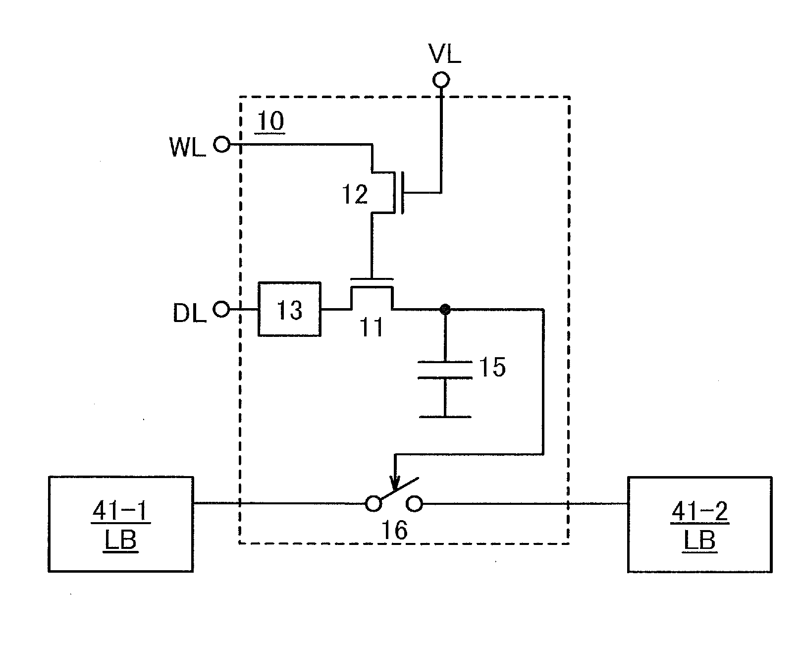
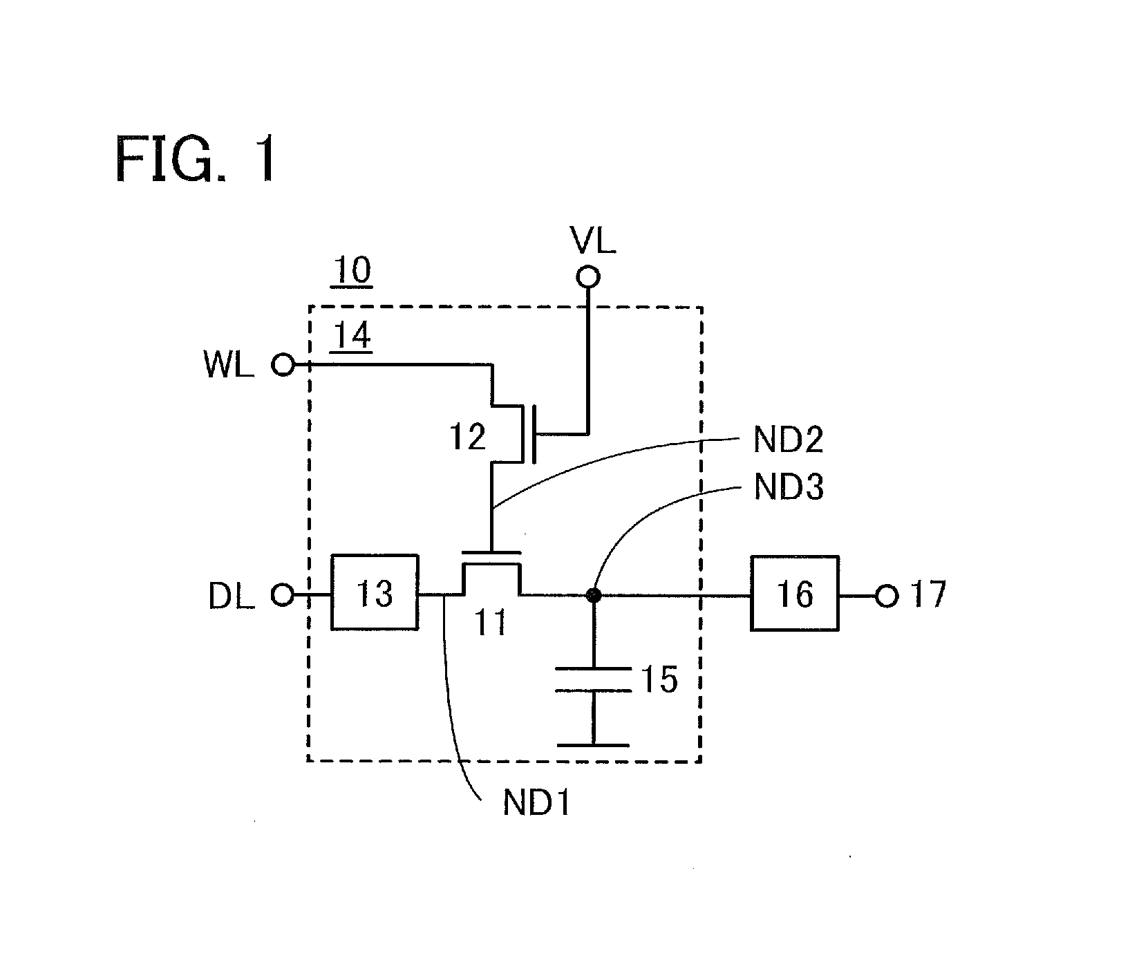
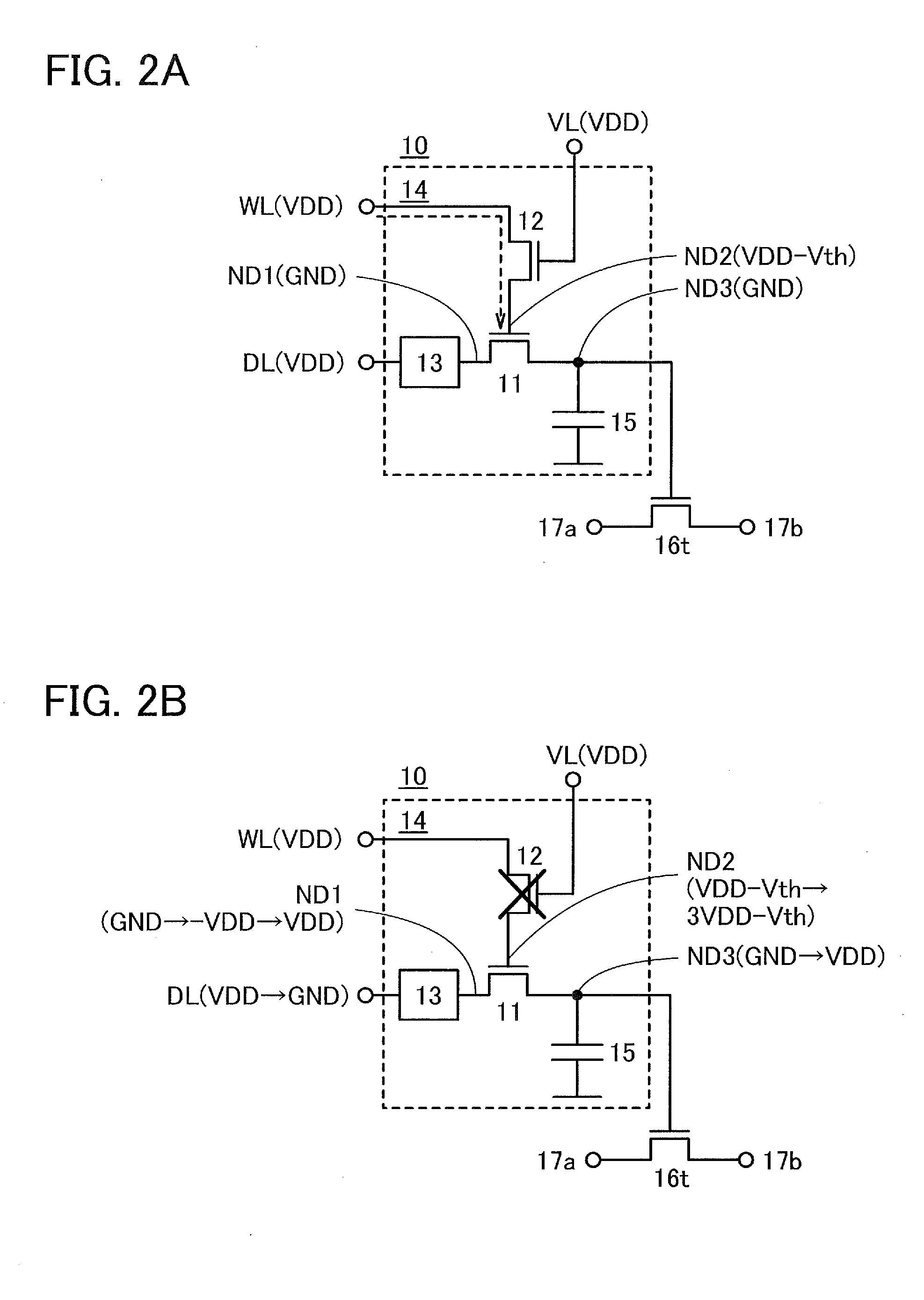
[0029]An embodiment of the present invention will be described in detail below with reference to the drawings. Note that the present invention is not limited to the following description. It will be readily appreciated by those skilled in the art that modes and details of the present invention can be modified in various ways without departing from the spirit and scope of the present invention. The present invention therefore should not be construed as being limited to the following description of the embodiment.

[0030]Note that a semiconductor device according to one embodiment of the present invention includes, in its category, a variety of semiconductor integrated circuits formed using semiconductor elements, such as microprocessors, image processing circuits, controllers for semiconductor display devices, digital signal processors (DSP), microcontrollers, control circuits for batteries such as secondary batteries, and protection circuits. The semiconductor device according to one ...


PUM


Abstract

A low-power storage device is provided. The storage device includes a first transistor, a second transistor, a logic element, and a semiconductor element. The second transistor controls supply of a first signal to a gate of the first transistor. When the potential of a second signal to be input is changed from a first potential into a second potential lower than the first potential, the logic element changes the potential of a first terminal of the first transistor from a third potential lower than the second potential into the first potential after the logic element changes the potential of the first terminal of the first transistor from the second potential into the third potential. The semiconductor element has a function of making a second terminal of the first transistor floating. The first transistor includes a channel formation region in an oxide semiconductor film.

Description

TECHNICAL FIELD[0001]One embodiment of the present invention relates to semiconductor devices. For example, one embodiment of the present invention relates to storage devices and semiconductor devices including the storage devices.BACKGROUND ART[0002]A metal oxide having semiconductor characteristics called an oxide semiconductor has attracted attention as a novel semiconductor. Transistors including oxide semiconductors are under development. For example, Patent Document 1 discloses the structure of a memory element for retaining data in a node that becomes floating by turning off such a transistor.REFERENCE[0003]Patent Document 1: Japanese Published Patent Application No. 2011-171702DISCLOSURE OF INVENTION[0004]To evaluate the performance of a semiconductor device such as a storage device, low power consumption and high-speed operation are important factors. However, when power supply voltage is decreased to reduce the power consumption of the storage device, the on-state current ...

Claims


Application Information

Patent Timeline
IPC IPC(8): H03K19/00
CPCH03K19/0013G11C11/403H03K19/1776
Inventor IKEDA, TAKAYUKI
Owner SEMICON ENERGY LAB CO LTD
Why Eureka
Try Eureka