
Ka-band high power amplifier structure having minimum processing and assembling errors
a high-power amplifier and assembly error technology, applied in amplifier combinations, amplifier types, coupling devices, etc., can solve the problems of reducing the power of parts, difficult to produce large power from a single part, and difficulty in designing and constructing circuits
- Summary
- Abstract
- Description
- Claims
- Application Information
AI Technical Summary
Benefits of technology
Problems solved by technology
Method used
Image

Examples
Embodiment Construction
[0057]Reference will now be made in greater detail to the present invention, exemplary embodiments of which are illustrated in the accompanying drawings. In the following description of the present invention, detailed descriptions of known functions and components incorporated herein will be omitted when they may make the subject matter of the present invention unclear.
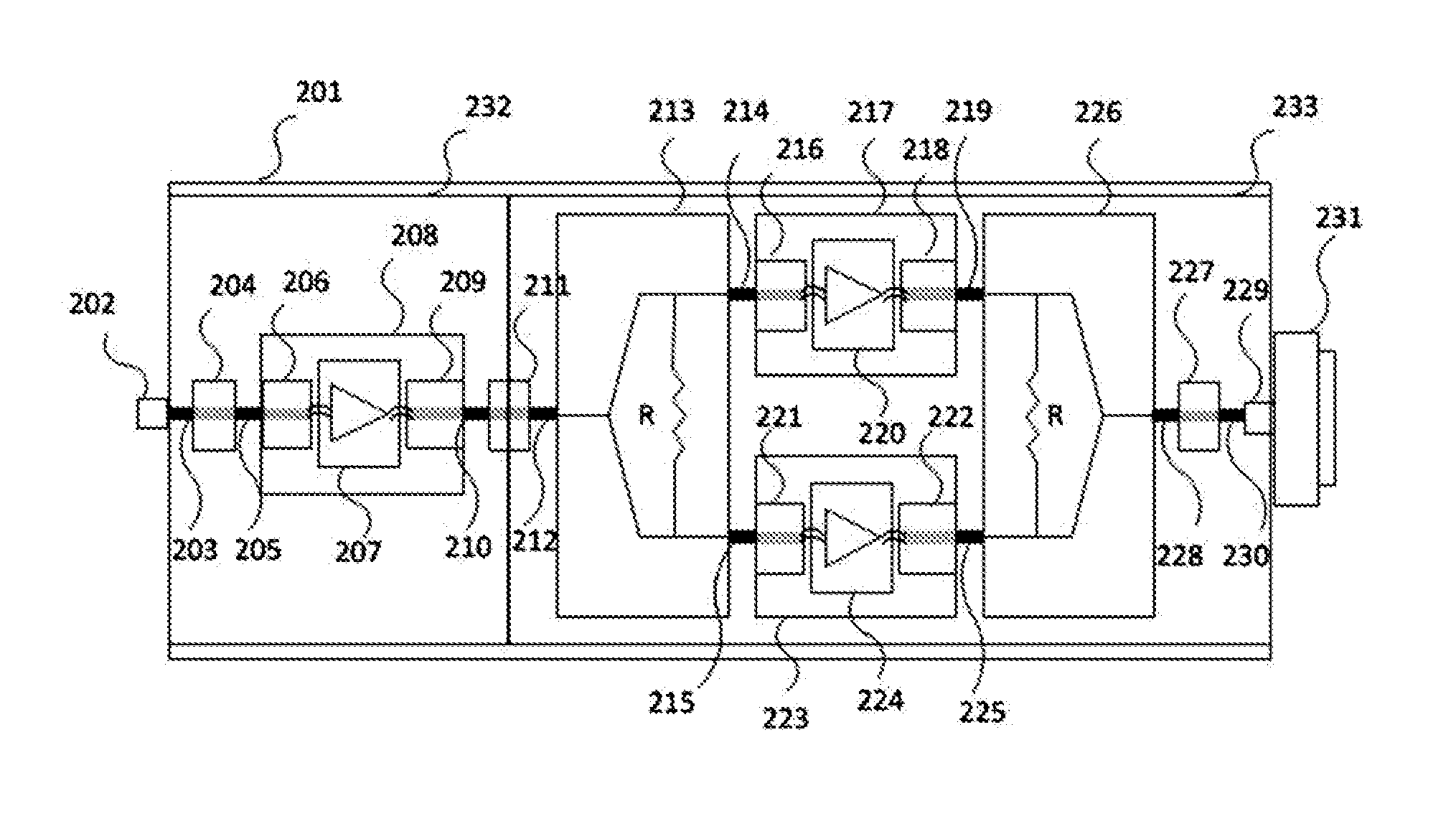
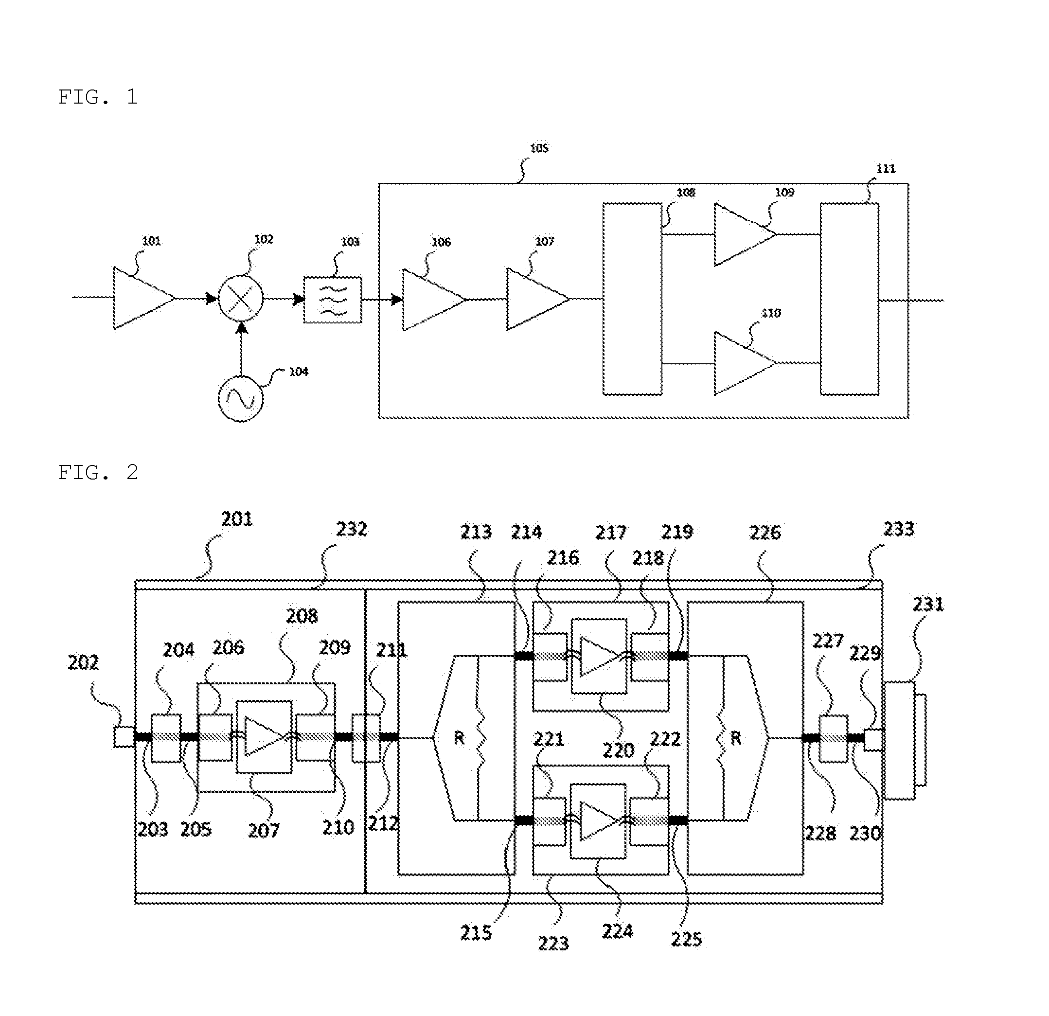
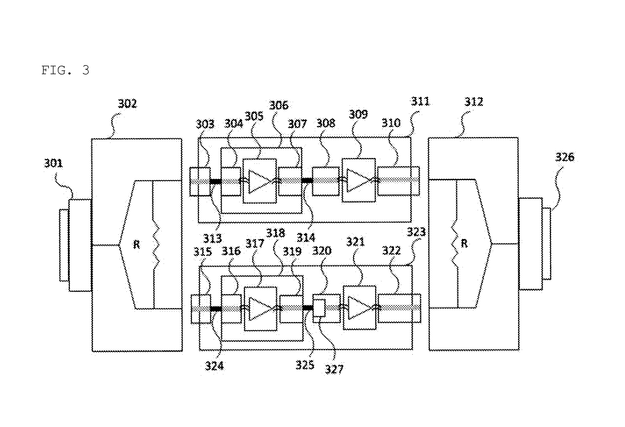
[0058]FIG. 3 is a view showing the configuration of a Ka-band high-power amplifier having a minimum processing and assembly error according to an embodiment of the present invention, FIG. 4 is a view showing the combining structure of a waveguide combiner of a Ka-band high-power amplifier having a minimum processing and assembly error according to an embodiment of the present invention, and FIG. 5 is a view showing the exterior of a final design of a Ka-band high-power amplifier having a minimum processing and assembly error according to an embodiment of the present invention.
[0059]Referring to FIG. 3 to FIG. 5, in or...
PUM
 Abstract
Description
Claims
Application Information