Photovoltaic devices and method of making

a technology of photovoltaic devices and manufacturing methods, applied in the direction of sustainable manufacturing/processing, final product manufacturing, vacuum evaporation coating, etc., can solve the problems of high defect density at the interface, and low conversion efficiency of thin film solar cells

Pending Publication Date: 2014-11-06
FIRST SOLAR INC (US)
View PDF19 Cites 18 Cited by
  • Summary
  • Abstract
  • Description
  • Claims
  • Application Information

AI Technical Summary

Problems solved by technology

However, thin film solar cells may have low conversion efficiencies.
Absorption of light by the window layer may be one of the phenomena limiting the conversion efficiency of a PV device.
Further, a lattice mismatch between the window layer and absorber layer (e.g., CdS / CdTe) layer may lead to high defect density at the interface, which may further lead to shorter interface carrier lifetime.
However, for most of the thin-film PV devices, if the window layer is too thin, a loss in performance can be observed due to low open circuit voltage (VOC) and fill factor (FF).

Method used


Image

  • Photovoltaic devices and method of making
  • Photovoltaic devices and method of making
  • Photovoltaic devices and method of making

Examples


example 1

Method of Manufacturing a Cadmium Telluride Photovoltaic Device Including a Graded CdTeSe Layer and No CdS Layer

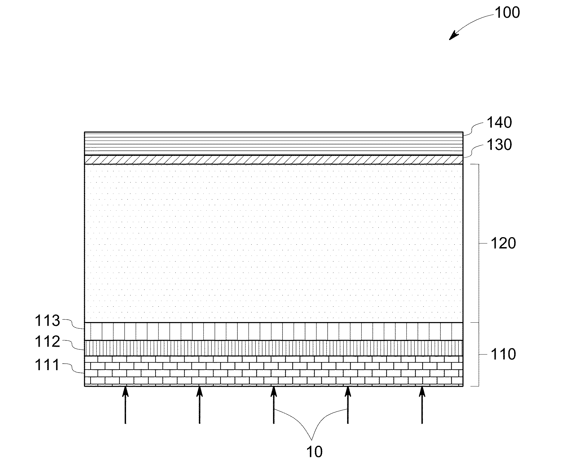
[0098]The method of making the photovoltaic device was similar to the Comparative Example 2, except after the step of interlayer formation, a 120 to 140 nanometers thick CdSe layer was sputtered on the interlayer, followed by deposition of CdTe layer (band gap=1.5 eV) on the CdSe layer (band gap=1.74 eV), and back contact formation.

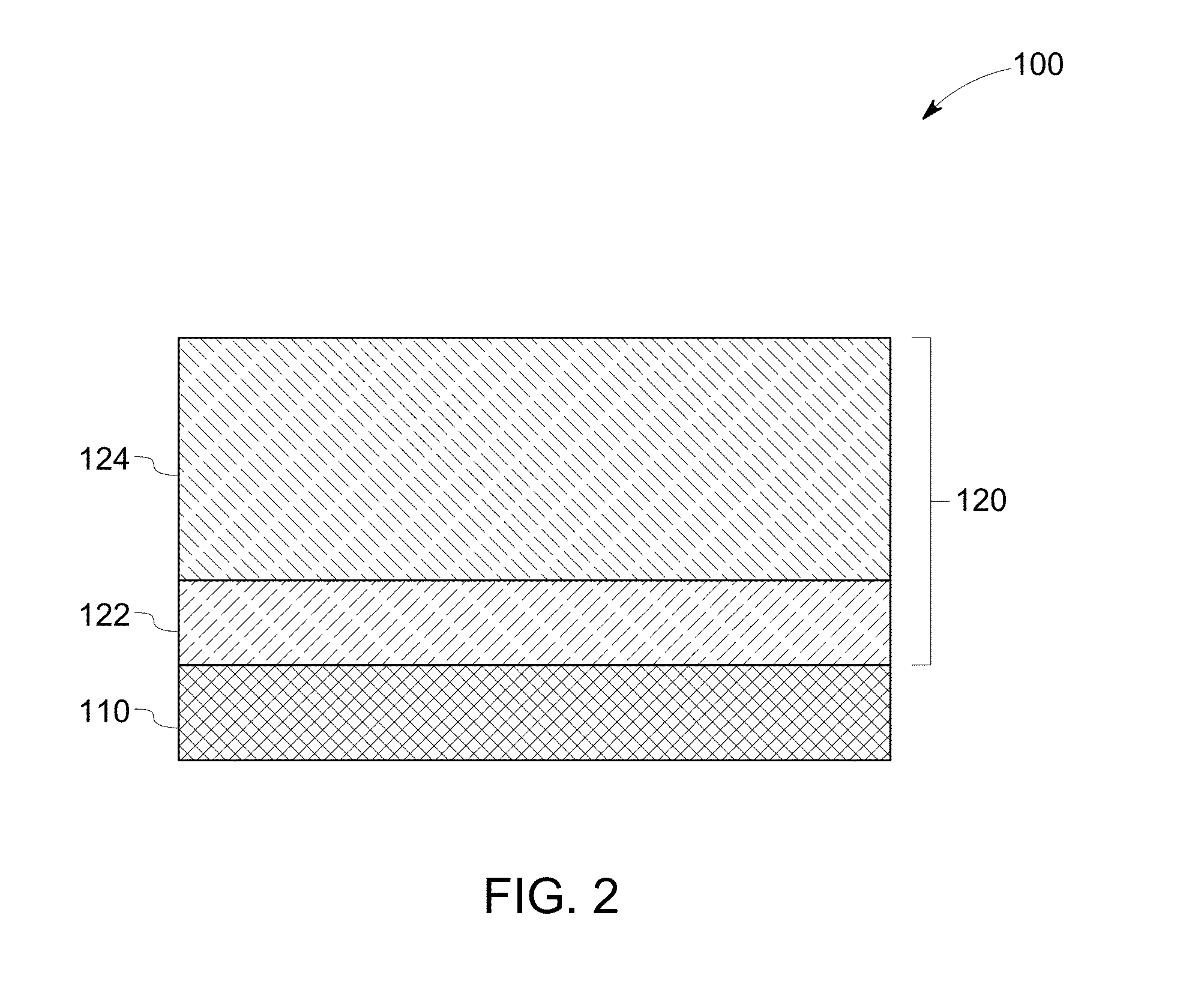
[0099]During device processing, the absorption edge of the composite CdSe / CdTe absorber appears to shift to energies that are lower than either pure CdTe or pure CdSe, as evidenced by a red shifted absorption edge as measured using wavelength dependence of the quantum efficiency (QE) of the solar cells (FIG. 12). This is consistent with extensive intermixing of the Te and Se within the absorber layer 120 thereby creating a lower band gap alloy. Further evidence of cadmium selenide telluride alloy formation is seen in photo-luminescence (PL) emis...


PUM

PropertyMeasurementUnit
thicknessaaaaaaaaaa
wavelengthaaaaaaaaaa
transparentaaaaaaaaaa

Abstract

A photovoltaic device is presented. The photovoltaic device includes a layer stack; and an absorber layer is disposed on the layer stack. The absorber layer comprises selenium, wherein an atomic concentration of selenium varies across a thickness of the absorber layer. The photovoltaic device is substantially free of a cadmium sulfide layer.

Description

BACKGROUND[0001]The invention generally relates to photovoltaic devices. More particularly, the invention relates to photovoltaic devices including selenium, and methods of making the photovoltaic devices.[0002]Thin film solar cells or photovoltaic (PV) devices typically include a plurality of semiconductor layers disposed on a transparent substrate, wherein one layer serves as a window layer and a second layer serves as an absorber layer. The window layer allows the penetration of solar radiation to the absorber layer, where the optical energy is converted to usable electrical energy. The window layer further functions to form a heterojunction (p-n junction) in combination with an absorber layer. Cadmium telluride / cadmium sulfide (CdTe / CdS) heterojunction-based photovoltaic cells are one such example of thin film solar cells, where CdS functions as the window layer.[0003]However, thin film solar cells may have low conversion efficiencies. Thus, one of the main focuses in the field ...

Claims


Application Information

Patent Timeline
Patent Type & Authority Applications(United States)
IPC IPC(8): H01L31/0296H01L31/0272
CPCH01L31/0296H01L31/0272H01L31/022466H01L31/02966H01L31/065H01L31/073Y02E10/50H01L21/0256H01L21/02562H01L31/02963H01L31/072H01L21/02422H01L21/02477H01L21/0248H01L21/02483H01L21/02491H01L21/02505H01L21/0251H01L31/03925H01L31/1836C23C14/0629H01L31/1832Y02E10/547Y02E10/543Y02P70/50
Inventor BLAYDES, HOLLY ANNANDREINI, KRISTIAN WILLIAMHUBER, WILLIAM HULLINGERHINNERS, EUGENE THOMASSHIANG, JOSEPH JOHNLIANG, YONGCHOI, JONGWOO
Owner FIRST SOLAR INC (US)
Why Eureka
Try Eureka