
Complementary metal oxide semiconductor power amplifier

a technology of metal oxide semiconductor and power amplifier, which is applied in the direction of amplifiers, amplifier types, amplifiers with semiconductor devices/discharge tubes, etc., can solve the problems of limiting the integration of transceiver and amplifier circuitry, and utilizing different substrates

Inactive Publication Date: 2014-11-06
MORFIS SEMICON
View PDF2 Cites 26 Cited by
  • Summary
  • Abstract
  • Description
  • Claims
  • Application Information

AI Technical Summary

Benefits of technology

The patent text discusses various complementary metal oxide semiconductor transistor power amplifier circuits for RF applications. These circuits can amplify signals of multiple modes and frequency bands through a single die device. The envelope signal from the baseband transceiver provides instantaneous voltage for the power amplifier. The patent also describes an RF front end circuit which includes a unified power amplifier module for high band and low band, as well as a band switch for signal management. The technical effect of the patent is to provide efficient and flexible amplification of RF signals for various applications.

Problems solved by technology

Conventional mobile handset transceivers typically do not generate sufficient power or have sufficient sensitivity for reliable communications standing alone.
Utilizing different substrates limited the integration of transceiver and amplifier circuitry, so existing power amplifiers are designed as separate individual components with its own packaging.
With the increasing number of different operating frequency bands and communications standards, however, utilizing separate power amplifier modules for each complicates circuit board layout and mobile handset design.
Alternatively, features may be removed, that is, the number of modes and bands handled by the handset may be reduced, thereby limiting the functionality thereof.

Method used


Image

  • Complementary metal oxide semiconductor power amplifier
  • Complementary metal oxide semiconductor power amplifier
  • Complementary metal oxide semiconductor power amplifier

Examples


Embodiment Construction

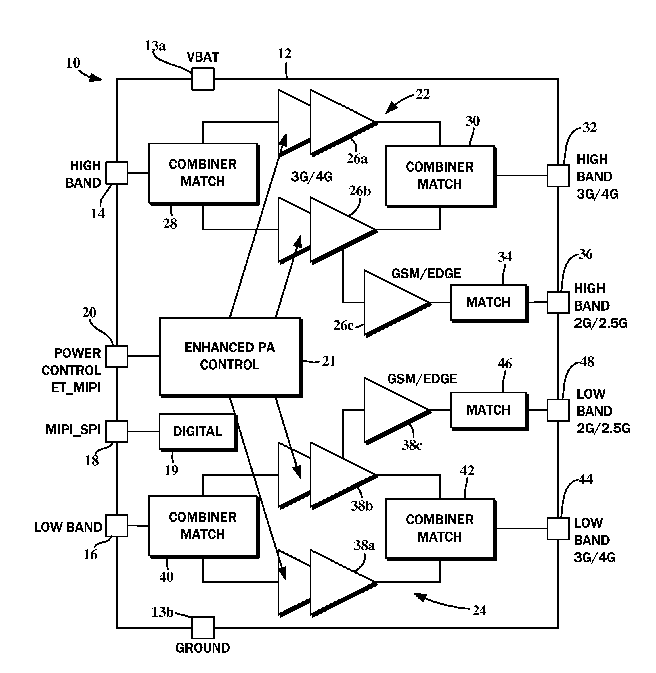
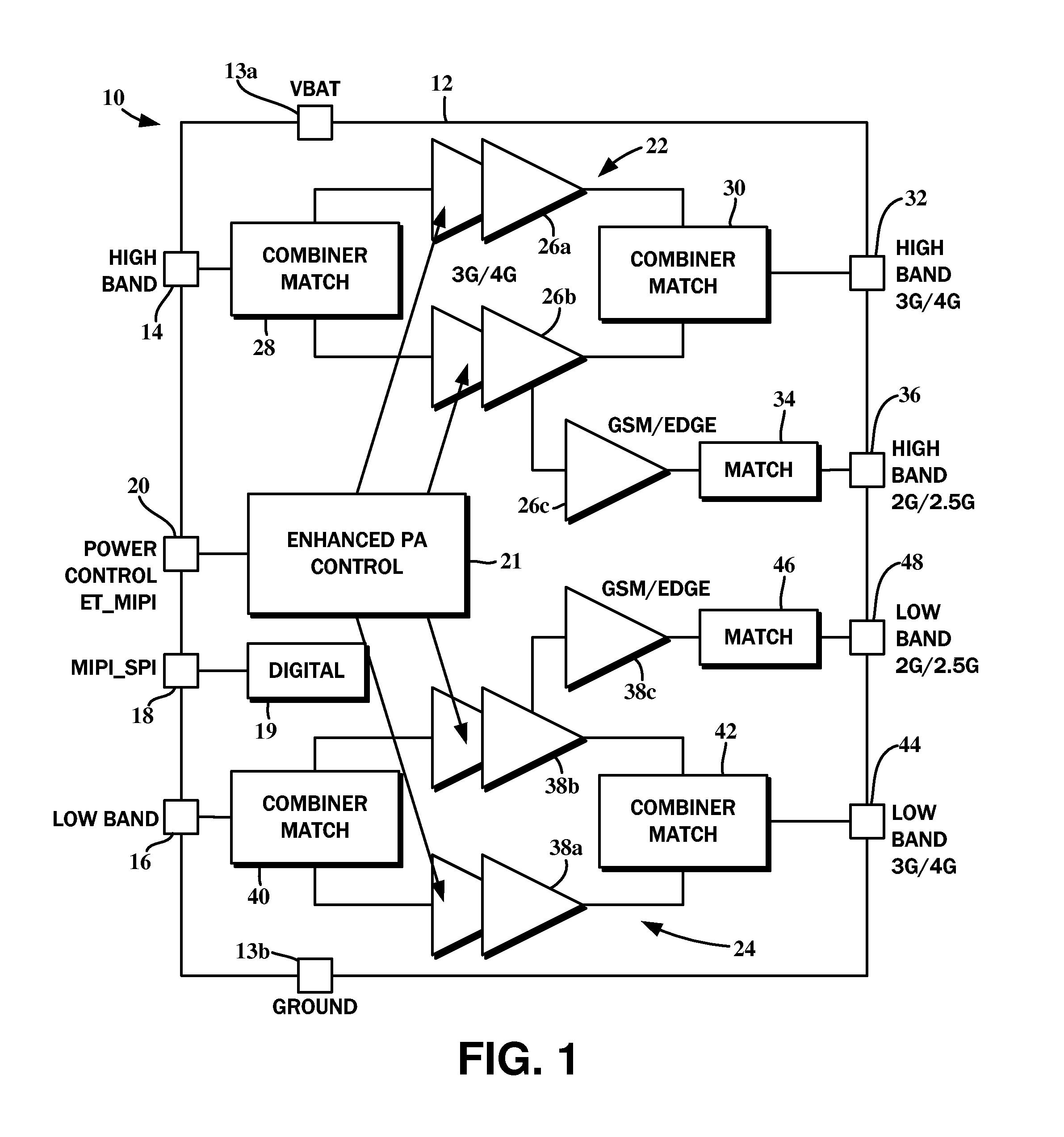
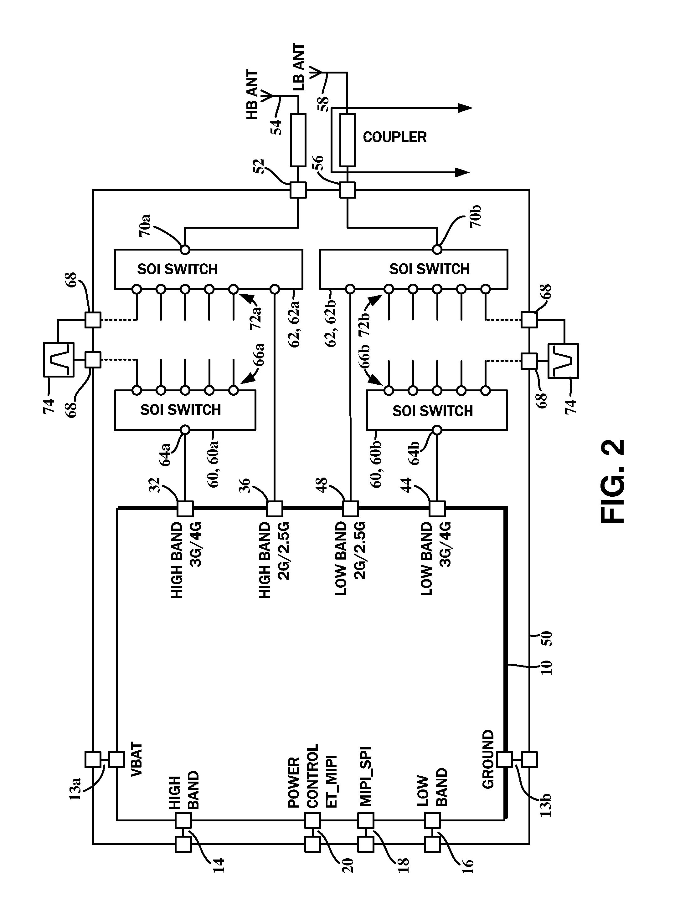
[0032]The present disclosure encompasses various embodiments of a power amplifier integrated circuit for amplifying mobile communications radio frequency (RF) signals of multiple modes and multiple bands, and is implemented on a single die with complementary metal oxide semiconductor transistors. An instantaneous voltage is provided to the power amplifiers as governed by an envelope signal from a baseband transceiver. The detailed description set forth below in connection with the appended drawings is intended as a description of the several presently contemplated embodiments of the architecture, and is not intended to represent the only form in which the disclosed invention may be developed or utilized. The description sets forth the functions and features in connection with the illustrated embodiments. It is to be understood, however, that the same or equivalent functions may be accomplished by different embodiments that are also intended to be encompassed within the scope of the ...


PUM


Abstract

An RF power amplifier circuit is disclosed. A driver amplifier stage includes a first set of a plurality of amplifier transistors in a cascode configuration, a driver amplifier stage input, and a driver amplifier stage output. A final amplifier stage includes a second set of a plurality of amplifier transistors in a cascode configuration, a final amplifier stage input connected to the driver amplifier stage output, a final amplifier stage output, and a power supply input. An envelope signal amplifier has an input connectible to an envelope signal source, and an output capacitively coupled to the power supply input. A power converter input is connected to the power supply input to provide supplemental power to the final amplifier stage based on an envelope signal from the envelope signal source that corresponds to an input RF signal.

Description

CROSS-REFERENCE TO RELATED APPLICATIONS[0001]This application relates to and claims the benefit of U.S. Provisional Application No. 61 / 819,465 filed May 3, 2013 and entitled “COMPLEMENTARY METAL OXIDE SEMICONDUCTOR POWER AMPLIFIER AND METHOD” the disclosure of which is wholly incorporated by reference in its entirety herein.STATEMENT RE: FEDERALLY SPONSORED RESEARCH / DEVELOPMENT[0002]Not ApplicableBACKGROUND[0003]1. Technical Field[0004]The present disclosure relates generally to radio frequency (RF) signal circuitry, and more particularly to complementary metal oxide semiconductor (CMOS) power amplifiers adapted for multi-mode, multi-band operation.[0005]2. Related Art[0006]Wireless communications systems find applications in numerous contexts involving information transfer over long and short distances alike, and there exists a wide range of modalities suited to meet the particular needs of each. Chief amongst these systems with respect to popularity and deployment is the mobile or...

Claims


Application Information

Patent Timeline
IPC IPC(8): H03F3/24H03F3/21H03F3/193
CPCH03F3/245H03F3/193H03F3/211H03F2200/451H03F2200/429H03F3/68H03F1/223
Inventor BALTEANU, FLORINEL
Owner MORFIS SEMICON
Learn More