Inverter Device

a technology of inverter and diode, which is applied in the direction of power conversion systems, pulse techniques, climate sustainability, etc., can solve the problems of increasing the loss and increasing the loss of reverse recovery in the diode, and achieve the effect of suppressing the ringing of the collector curren

Inactive Publication Date: 2014-11-13
HITACHI LTD
View PDF4 Cites 22 Cited by
  • Summary
  • Abstract
  • Description
  • Claims
  • Application Information

AI Technical Summary

Benefits of technology

[0024]According to the present invention, an inverter device can be provided that can suppress ringing of a collector current even in a case where a unipolar type diode is employed as a return current diode

Problems solved by technology

For this reason, there are drawbacks in that this reverse recovery current increases the loss that occurs when the power semiconductor switching element is turned ON (hereinafter referred to as turn ON loss Eon) and increases the reverse recovery loss that occurs in the diode when the return current diode is reversely recovered (hereinafter referred to as recovery loss Err).

Method used


Image

  • Inverter Device
  • Inverter Device
  • Inverter Device

Examples


first embodiment

Configuration of Inverter Device

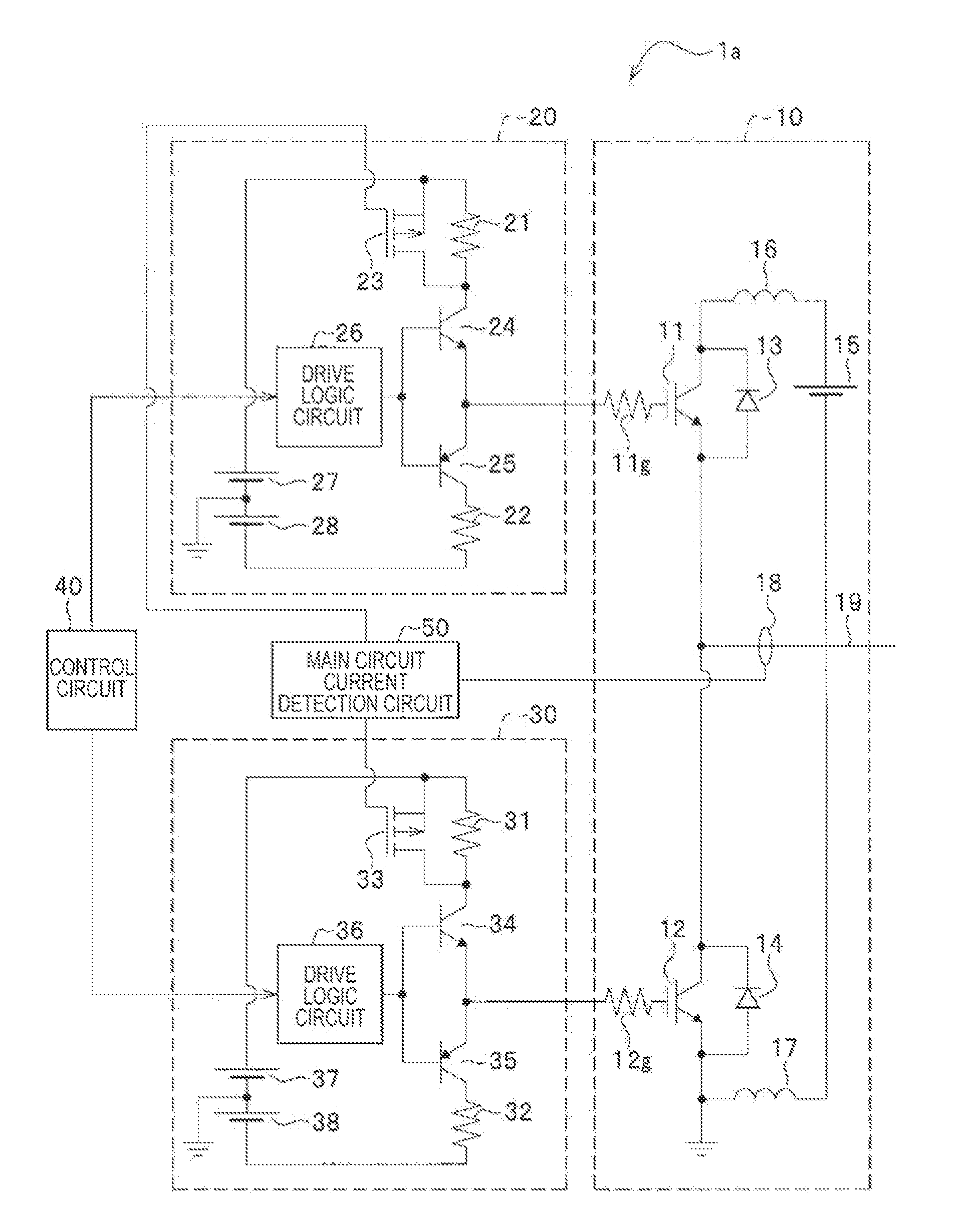
[0038]FIG. 1 is a configuration diagram illustrating an inverter device according to the first embodiment of the present invention. In general, an inverter device is constituted by a full-bridge circuit, but for the sake of explanation of the present embodiment, FIG. 1 illustrates an inverter device of a half bridge circuit.

[0039]First, a configuration of an inverter device according to the first embodiment of the present invention will be explained. As shown in FIG. 1, an inverter device 1a includes an inverter main circuit 10, an upper arm drive / control circuit 20, a lower arm drive / control circuit 30, a control circuit 40, and a main circuit current detection circuit 50.

[0040]The inverter main circuit 10 includes Si-IGBTs (Silicon Insulated Gate Bipolar Transistors) 11, 12 which are two power semiconductor switching elements connected in series, gate resistors 11g, 12g, unipolar type diodes 13, 14 connected in antiparallel to the Si-IGBTs 11, 12, r...

second embodiment

[0068]FIG. 7 is a configuration diagram illustrating an inverter device according to the second embodiment of the present invention. An inverter device 1b according to the second embodiment as shown in FIG. 7 has the same reference numerals denoting the same constituent elements as those of the inverter device 1a according to the first embodiment as shown in FIG. 1. The inverter device 1b according to the second embodiment is different from the inverter device 1a according to the first embodiment in that a control signal line 51 is connected from a main circuit current detection circuit 50 to a control circuit 40.

[0069]More specifically, in the inverter device 1a according to the first embodiment, the main circuit current detection circuit 50 changes the gate resistance value of the power semiconductor switching element (i.e., Si-IGBTs 11, 12) on the basis of the magnitude of the main circuit current detected by the main circuit current detection current transformer 18, thus suppres...

third embodiment

[0081]FIG. 9 is a configuration diagram illustrating an inverter device according to the third embodiment of the present invention. An inverter device 1c according to the third embodiment as shown in FIG. 9 has the same reference numerals denoting the same constituent elements as those of the inverter device 1b according to the second embodiment as shown in FIG. 7. The inverter device 1c according to the third embodiment is different from the inverter device 1b according to the second embodiment in that the gate resistance value (gate impedance) of the power semiconductor switching element is switched to three levels.

[0082]First, the configuration of the inverter device 1c according to the third embodiment as illustrated in FIG. 9 will be explained without repeated explanation. As shown in FIG. 9, the inverter device 1c the according to the third embodiment of the present invention includes an inverter main circuit 10, an upper arm drive / control circuit 20a, a lower arm drive / contro...


PUM


Abstract

In a switching circuit in which a power semiconductor switching element and a unipolar type diode are connected in parallel, the noise due to ringing is reduced. When the main circuit current flowing is equal to or less than a predetermined value, an Si-IGBT is switched and driven by a gate resistance. In this case, when the main circuit current detected is equal to or more than a threshold value, a main circuit current detection circuit changes a gate resistance switching pMOS from ON state to OFF state. Accordingly, the Si-IGBT operates with a summation of a gate resistance and a gate resistor. More specifically, a gate resistance value of a gate drive circuit of the Si-IGBT increases. Therefore, dv / dt of the collector-emitter voltage of the Si-IGBT, i.e., the recovery dv / dt of the unipolar type diode, is small, and therefore, the noise due to ringing can be reduced.

Description

TECHNICAL FIELD[0001]The present invention relates to an inverter device having a semiconductor module in which a semiconductor switching element and a diode are connected in an antiparallel manner, and more particularly, to an inverter device which drives, using the gate, a power semiconductor module in which a power semiconductor switching element is connected in antiparallel to a diode which is a unipolar device made of a wide gap semiconductor such as silicon carbide and gallium nitride.BACKGROUND ART[0002]In recent years, semiconductor elements using materials such as silicon carbide (hereinafter referred to as SiC) and gallium nitride (hereinafter referred to as GaN) as a wide gap semiconductor element in which the width of the band gap area having no electrons is wide are attracting attention. These materials have breakdown voltage strengths about ten times as high as that of silicon (hereinafter referred to as Si) used as a material of a generally-available semiconductor ele...

Claims


Application Information

Patent Timeline
Patent Type & Authority Applications(United States)
IPC IPC(8): H02M1/08H02M7/5387
CPCH02M1/08H02M7/5387H02M7/53803H03K17/166H03K17/168H03K2217/0036Y02B70/10H02M1/0032
Inventor KATOH, KAORUISHIKAWA, KATSUMIOGAWA, KAZUTOSHI
Owner HITACHI LTD
Why Eureka
Try Eureka