Solid-state imaging device, driving method for solid-state imaging device, and electronic appliance

a solid-state imaging and driving method technology, applied in the direction of radio frequency controlled devices, instruments, television systems, etc., can solve the problems of difficult to reduce the size, poor simultaneity of the exposure time in the pixel region, and distorted images obtained by photographing a moving subject, so as to achieve improved saturation charge amount and higher image quality

Active Publication Date: 2014-11-27
SONY SEMICON SOLUTIONS CORP
View PDF10 Cites 84 Cited by
  • Summary
  • Abstract
  • Description
  • Claims
  • Application Information

AI Technical Summary

Benefits of technology

[0023]According to the solid-state imaging device of the present disclosure, since the first charge accumulation unit and the second charge accumulation unit are stacked in the substrate depth direction, the pixels are miniaturized. Moreover, since

Problems solved by technology

This row-sequential scanning causes time displacement in an accumulation period for each pixel row, thereby causing a phenomenon called focal plane distortion that the image obtained by photographing a moving subject is distorted.
In the case of performing the global exposure with the mechanical shutter, however, a mechanical light-shielding means is necessary, which makes it difficult to reduce the size.
Further, since there is a limitation in mechanical driving speed of the mechanical shutter, the simultaneity of the exposure time in the pixel region is poor.
This causes problems that the signal charges held in the floating diffusion until the readout time leak out or deteriorate due to noise (referred to as alias) that is generated by the photoelectric conversion of the floating diffusion.
The provision of the light-shielding film, however, causes problems that the sensitivity deteriorates because the openi

Method used


Image

  • Solid-state imaging device, driving method for solid-state imaging device, and electronic appliance
  • Solid-state imaging device, driving method for solid-state imaging device, and electronic appliance
  • Solid-state imaging device, driving method for solid-state imaging device, and electronic appliance

Examples


first embodiment

1. solid-state imaging device of back-illumination type

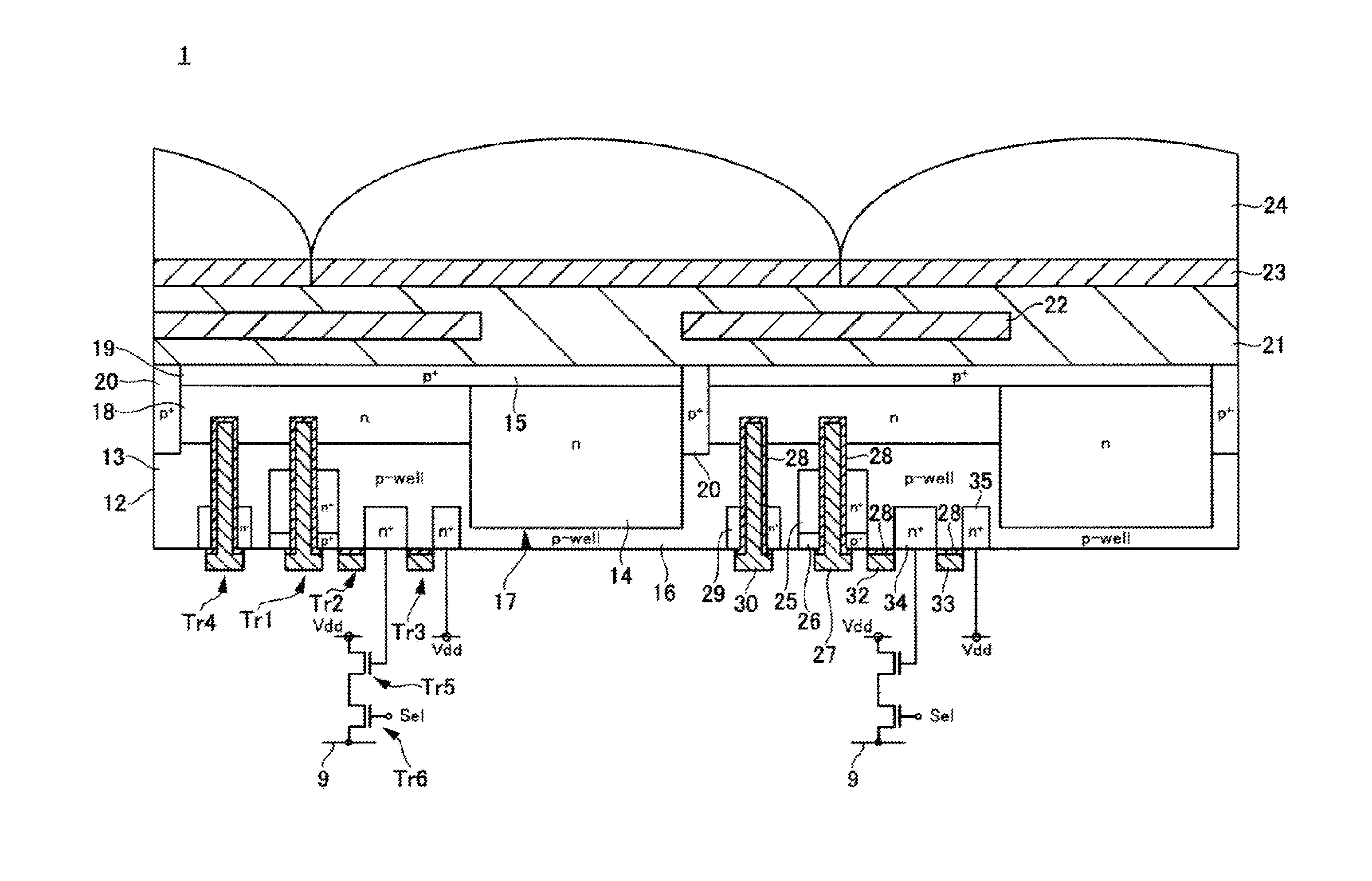
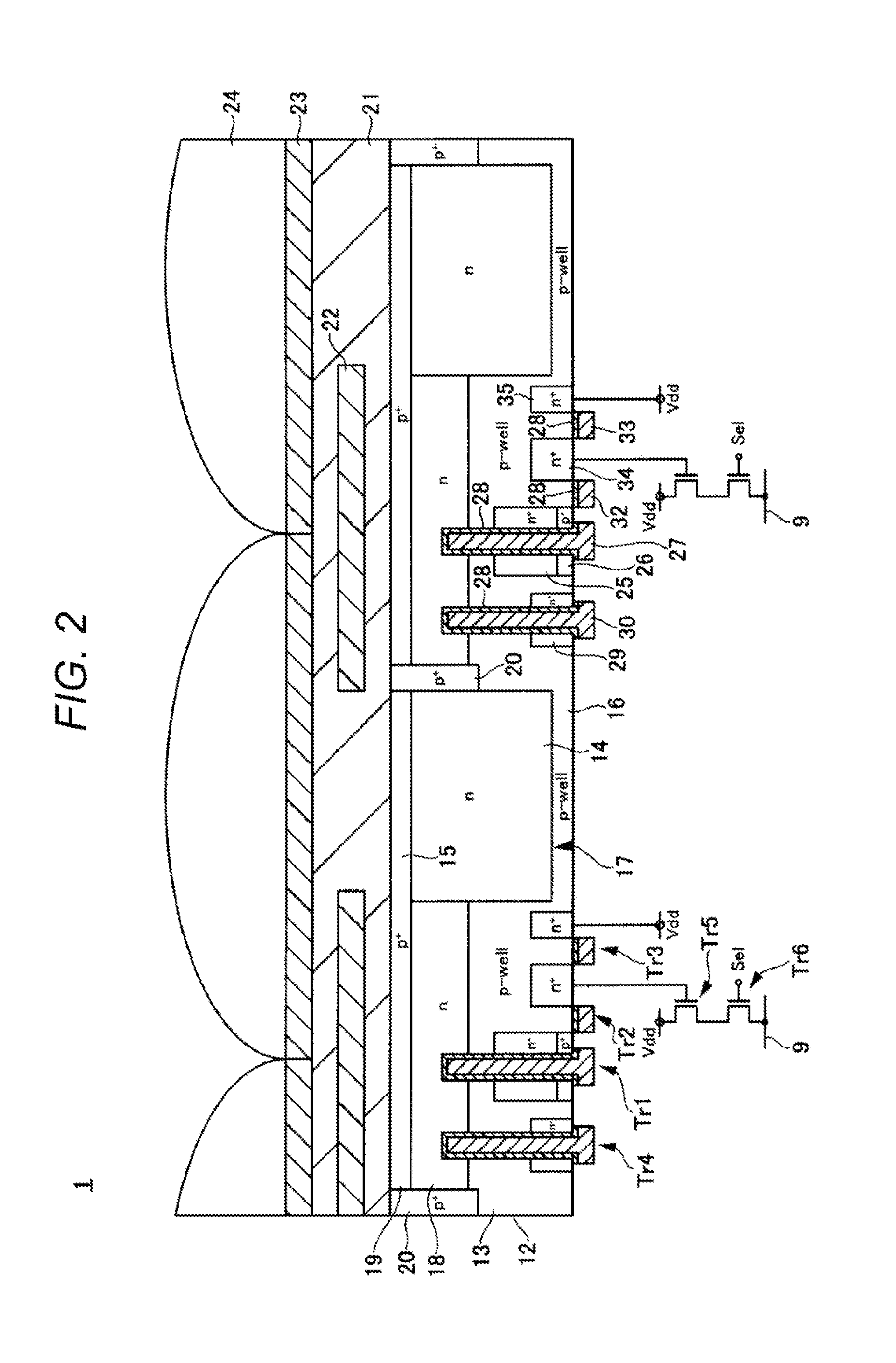
[0054]1-1 Structure of solid-state imaging device

[0055]1-2 Structure of main components

[0056]1-3 Manufacturing method

[0057]1-4 Driving method

[0058]1-5 Modified example

2. Second embodiment: example of structuring one vertical transistor in each pixel

3. Third embodiment: solid-state imaging device of front-illumination type

4. Fourth embodiment: example of drifting signal charges in transfer electrode

5. Fifth embodiment: example of reading out signal charges in a signal readout transistor

6. Sixth embodiment: example of stacking photoelectric conversion unit on substrate

[0059]6-1 Structure of main components

[0060]6-2 Manufacturing method

[0061]6-3 Driving method

[0062]6-4 First modified example

[0063]6-5 Second modified example

7. Seventh embodiment: example of providing p-type semiconductor layer on upper layer of photoelectric conversion unit

[0064]7-1 Structure of main components

[0065]7-2 Manufacturing method

8. Eighth embodiment: exa...

second embodiment

2. Second Embodiment

Example of Forming One Vertical Transistor in Each Pixel

[0135]Next, a solid-state imaging device according to a second embodiment of the present disclosure is described. FIG. 8 is a sectional structural diagram of main components of a solid-state imaging device 70 according to this embodiment. In FIG. 8, the same part as that of FIG. 2 is denoted by the same reference symbol and the description thereto is not repeated.

[0136]This embodiment describes an example in which the second reset transistor Tr4 is not formed in the solid-state imaging device 1 according to the first embodiment. In other words, each pixel of the solid-state imaging device 70 of this embodiment includes the first transfer transistor Tr1, the second transfer transistor Tr2, the reset transistor Tr3, the amplification transistor Tr5, and the selection transistor Tr6.

[0137]FIG. 9 is an equivalent circuit diagram of the pixel of the solid-state imaging device 70 of this embodiment. As illustrated...

third embodiment

3. Third Embodiment

Solid-State Imaging Device of Front-Illumination Type

[0149]Next, a solid-state imaging device according to a third embodiment of the present disclosure is described. Since the overall structure of the solid-state imaging device according to this embodiment is similar to that of FIG. 1, the illustration is omitted and the overlapping description is omitted. FIG. 11 is a sectional structure diagram of main components of a solid-state imaging device 71 of this embodiment. This embodiment describes an example of a solid-state imaging device of front-illumination type, in which the light incidence surface is formed on the opposite side to that of the solid-state imaging device 1 of the first embodiment. In FIG. 11, the same part as that in FIG. 2 is denoted by the same reference symbol and the description thereto is not repeated. Note that in FIG. 11, the illustration of a part of the pixel transistors included in each pixel is omitted.

[0150]In the solid-state imaging ...


PUM


Abstract

The present disclosure relates to a solid-state imaging device, a driving method for the same, and an electronic appliance, and an object is to provide a solid-state imaging device that can achieve the pixel miniaturization and the global shutter function with higher sensitivity and saturated charge amount. Another object is to provide an electronic appliance including the solid-state imaging device. In a solid-state imaging device 1 having the global shutter function, a first charge accumulation unit 18 and a second charge accumulation unit 25 are stacked in the depth direction of a substrate 12, and the transfer of the signal charges from the first charge accumulation unit 12 to the second charge accumulation unit 25 is conducted by a vertical first transfer transistor Tr1. Thus, the pixel miniaturization can be achieved.

Description

TECHNICAL FIELD[0001]The present disclosure relates to a solid-state imaging device, and particularly to a CMOS solid-state imaging device and a driving method for the same. Moreover, the present disclosure relates to an electronic appliance including the solid-state imaging device.BACKGROUND ART[0002]A general CMOS (Complementary Metal Oxide Semiconductor) solid-state imaging device has a mechanism in which a pixel array arranged two-dimensionally is scanned sequentially for each pixel row to read out pixel signals. This row-sequential scanning causes time displacement in an accumulation period for each pixel row, thereby causing a phenomenon called focal plane distortion that the image obtained by photographing a moving subject is distorted.[0003]In the photographing of a subject moving fast, for which such image distortion is not allowed, or in the application of sensing in which the simultaneity of the photographed image is necessary, the global shutter function or the mechanica...

Claims


Application Information

Patent Timeline
IPC IPC(8): H01L27/146H04N5/374
CPCH01L27/14638H04N5/374H01L27/14643H01L27/14603H01L27/14609H01L27/14623H01L27/1464H01L27/14689H01L27/14605H01L27/14612H01L27/14621H01L27/14627H04N25/616H04N25/771H04N25/77H04N25/76
Inventor TODA, ATSUSHI
Owner SONY SEMICON SOLUTIONS CORP
Why Eureka
Try Eureka