Multi-layer conversion material for down conversion in solid state lighting

a conversion material and solid-state lighting technology, applied in the field of solid-state light sources, can solve the problems of high-efficiency light sources, pollution of the environment, and loss of as much as 95% of input energy, and achieve the effects of reducing the amount of costly conversion materials, improving emission intensity and color rendering index, and improving the quality of leds

Active Publication Date: 2014-12-18
CREELED INC
View PDF18 Cites 38 Cited by
  • Summary
  • Abstract
  • Description
  • Claims
  • Application Information

AI Technical Summary

Benefits of technology

[0013]The present invention is directed to different LEDs having conversion materials arranged in a layered fashion to improve the LEDs' characteristics. Some of these characteristics include improved emission intensity and color rendering index (CRI), while others can include a reduction in the amount of costly conversion material needed to reach a desired color point or CRI. In some embodiments the different conversion material layers can be arranged so that respective layers absorb light from the LED light source and re-emit light in different wavelength spectrum. In some embodiments, the layers can be tailored so that there is minimal overlap of the emission and excitation spectrums for the conversion materials in the layers.

Problems solved by technology

However, such lamps are highly inefficient light sources, with as much as 95% of the input energy lost, primarily in the form of heat or infrared energy.
Compact Fluorescent Lamps are more effective than incandescent at converting the electricity into light but require the use of toxic materials such as Hg such that when the lamps are disposed of these toxic materials that can pollute the environment, including underground water supplies.
While the reflective cup 13 may direct light in an upward direction, optical losses may occur when the light is reflected (i.e. some light may be absorbed by the reflective cup due to the less than 100% reflectivity of practical reflector surfaces).
In addition, heat retention may be an issue for a package such as the package 10 shown in FIG. 1a, since it may be difficult to extract heat through the leads 15A, 15B.
One disadvantage of mixing the phosphors together is that there can be significant “cross-talk” or “overlap” between the emission and excitation spectrum for the different phosphors, which can negatively impact the CRI and emission efficiency for the combined emitted light. FIG. 3 shows graphs 30 showing one example of the emission and excitation characteristics for conventional phosphors that can be mixed together.
There is also some efficiency loss associated with the phosphor absorption and emission process, and repeating this process through re-absorption of the yellow / green light by the red phosphor results in additional efficiency losses.

Method used


Image

  • Multi-layer conversion material for down conversion in solid state lighting
  • Multi-layer conversion material for down conversion in solid state lighting
  • Multi-layer conversion material for down conversion in solid state lighting

Examples


Embodiment Construction

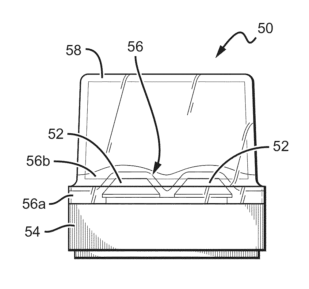
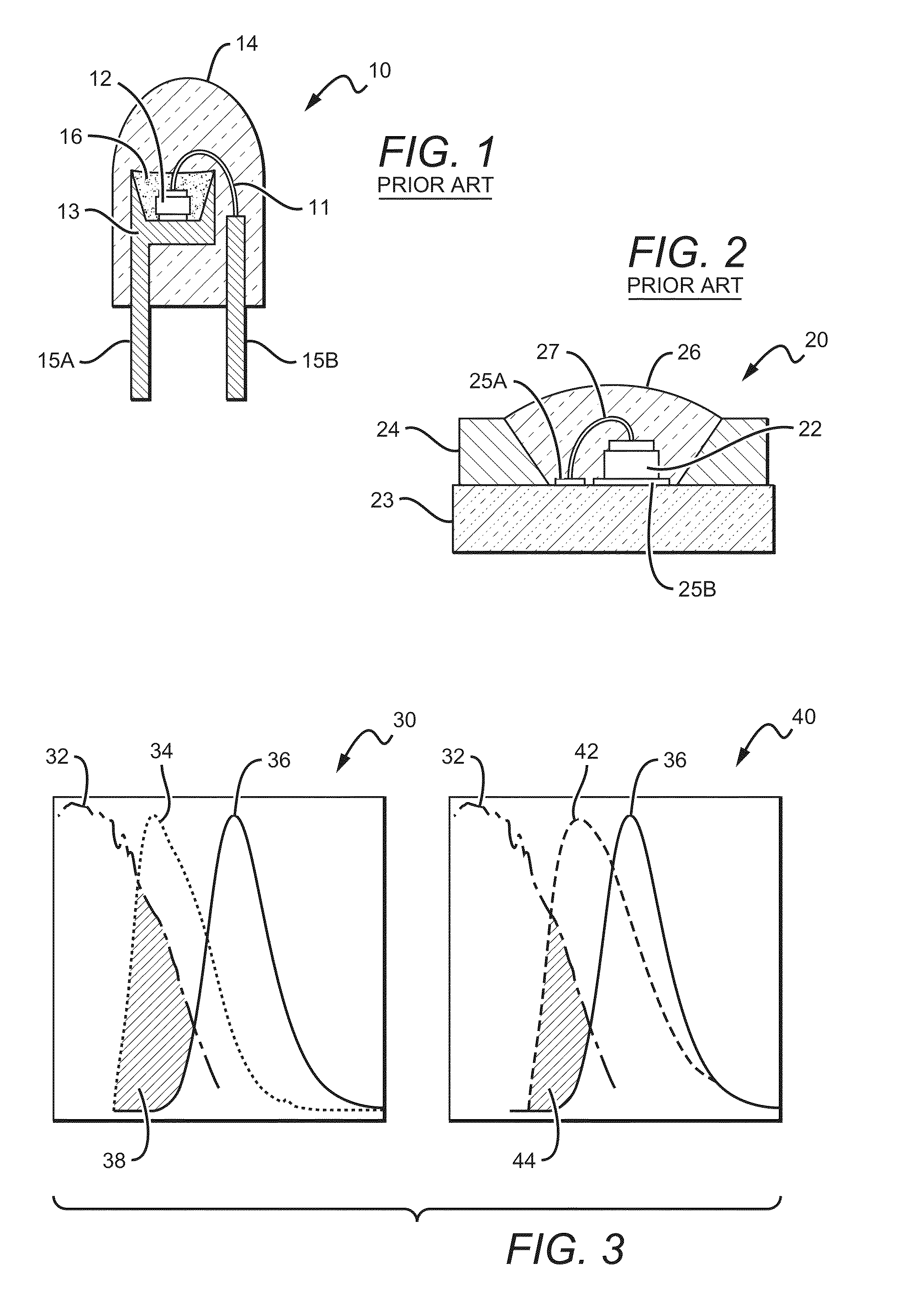
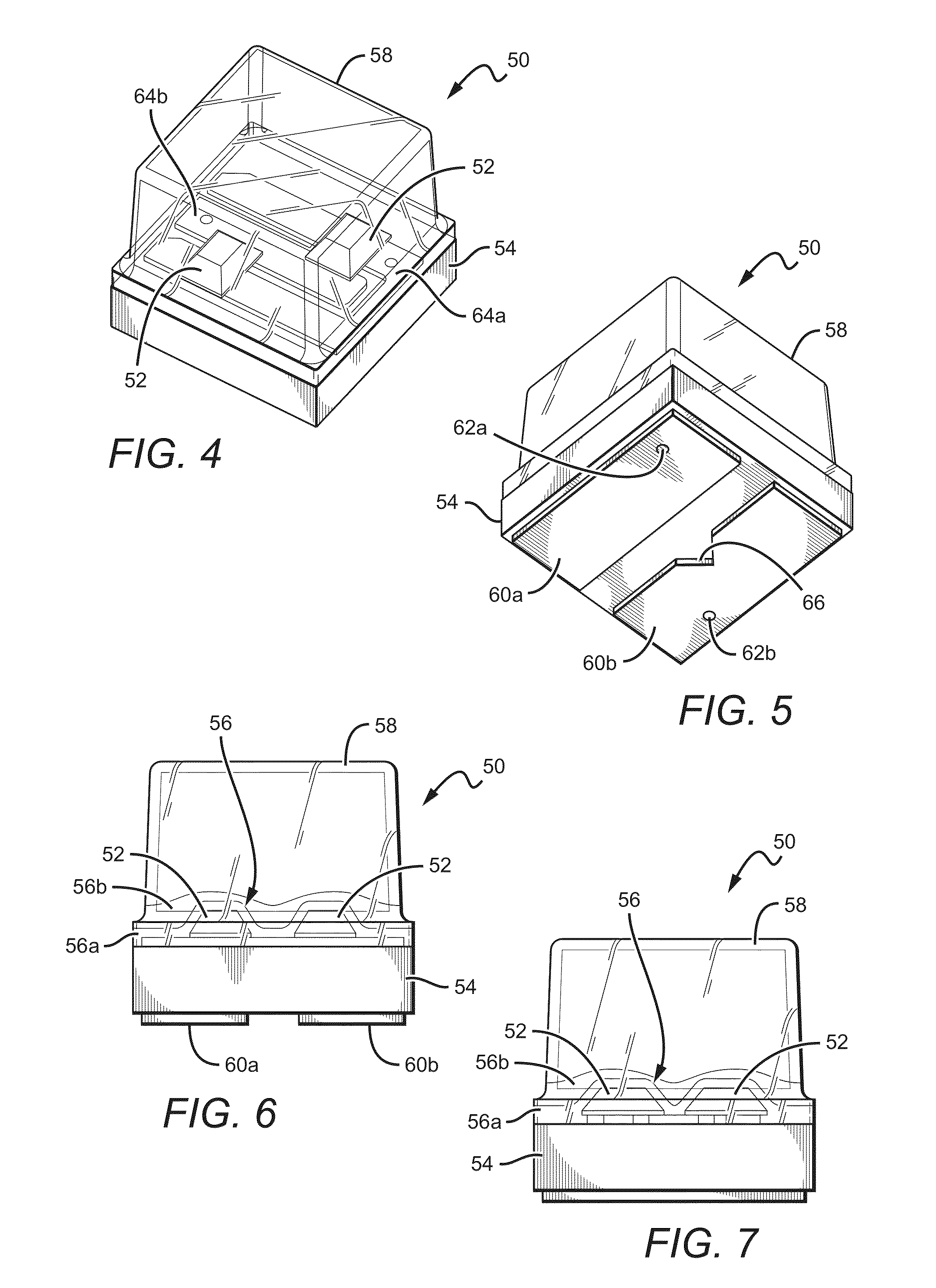
[0043]The present invention is directed to solid state emitters, such as light emitting diodes (LED or LEDs) that utilize multiple conversion materials or phosphor types in the conversion process in order to achieve the desired emission color point. Different embodiments of the present invention can apply the different phosphor types in separate layers on, above or around one or a plurality of LED chips to achieve the desired light down conversion. The LEDs can then emit a desired combination of light from the LED chips and conversion material, such as a white light combination.

[0044]In some embodiments, one or more of the phosphor layer can be a relatively thin conformal layer having a substantially uniform phosphor particle density. In other embodiments, a phosphor layer may be provided that comprises phosphor particles that are nonuniformly dispersed therein. In some embodiments the layers can have a phosphor-free regions in different locations, such as at the exterior surfaces o...


PUM

PropertyMeasurementUnit
thicknessaaaaaaaaaa
thicknessaaaaaaaaaa
peak wavelengthaaaaaaaaaa

Abstract

Light emitting diodes are disclosed that utilize multiple conversion materials in the conversion process in order to achieve the desired emission color point. Different embodiments of the present invention can comprise different phosphor types in separate layers on, above or around one or a plurality of LED chips to achieve the desired light conversion. The LEDs can then emit a desired combination of light from the LED chips and conversion material. In some embodiments, conversion materials can be applied as layers of different phosphor types in order of longest emission wavelength phosphor first, followed by shorter emission phosphors in sequence as opposed to applying in a homogeneously mixed phosphor converter. The conversion material layers can be applied as a blanket over the LED chips and the area surrounding the chip, such as the surface of a submount holding the LED chips.

Description

[0001]This application is a continuation of and claims the benefit of U.S. patent application Ser. No. 13 / 028,863, to Tong et al., filed on Feb. 16, 2011, and U.S. patent application Ser. No. 13 / 649,052, to Lowes et al., filed on Oct. 10, 2012.BACKGROUND OF THE INVENTION[0002]1. Field of the Invention[0003]This invention relates to solid state light sources and in particular to efficient and reliable light emitting diode (LED) packages having enhanced emission characteristics through separation of different phosphor components.[0004]2. Description of the Related Art[0005]Incandescent or filament-based lamps or bulbs are commonly used as light sources for both residential and commercial facilities. However, such lamps are highly inefficient light sources, with as much as 95% of the input energy lost, primarily in the form of heat or infrared energy. Compact Fluorescent Lamps are more effective than incandescent at converting the electricity into light but require the use of toxic mat...

Claims


Application Information

Patent Timeline
Patent Type & Authority Applications(United States)
IPC IPC(8): H01L25/075H01L33/54H01L33/60H01L33/50
CPCH01L25/0753H01L33/507H01L33/60H01L33/54H01L33/504F21K9/232F21K9/64F21V3/02F21V3/12F21Y2113/13F21Y2115/10H01L2224/32245H01L2224/48091H01L2224/48227H01L2224/48247H01L2224/73265H01L2924/0002H01L2924/181H01L33/62H01L33/505H01L2933/0041H01L2924/00H01L2924/00012H01L2924/00014F21V5/00F21V9/08
Inventor ZHANG, FANIBBETSON, JAMESKELLER, BERNDLOWES, THEODOREVAN DE VEN, ANTONYKIRCHER, DEBORAHGILBERT, TAO
Owner CREELED INC
Why Eureka
Try Eureka