

Rectifier circuit
a rectifier circuit and loss reduction technology, applied in the direction of ac-dc conversion without reversal, power conversion systems, electrical equipment, etc., can solve the problems of reducing the overall efficiency of the device, reducing the cost of fast recovery diodes, and increasing the cost of rectifying diodes. , to achieve the effect of low cost and loss reduction
- Summary
- Abstract
- Description
- Claims
- Application Information
AI Technical Summary
Benefits of technology
Problems solved by technology
Method used
Image

Examples
first embodiment
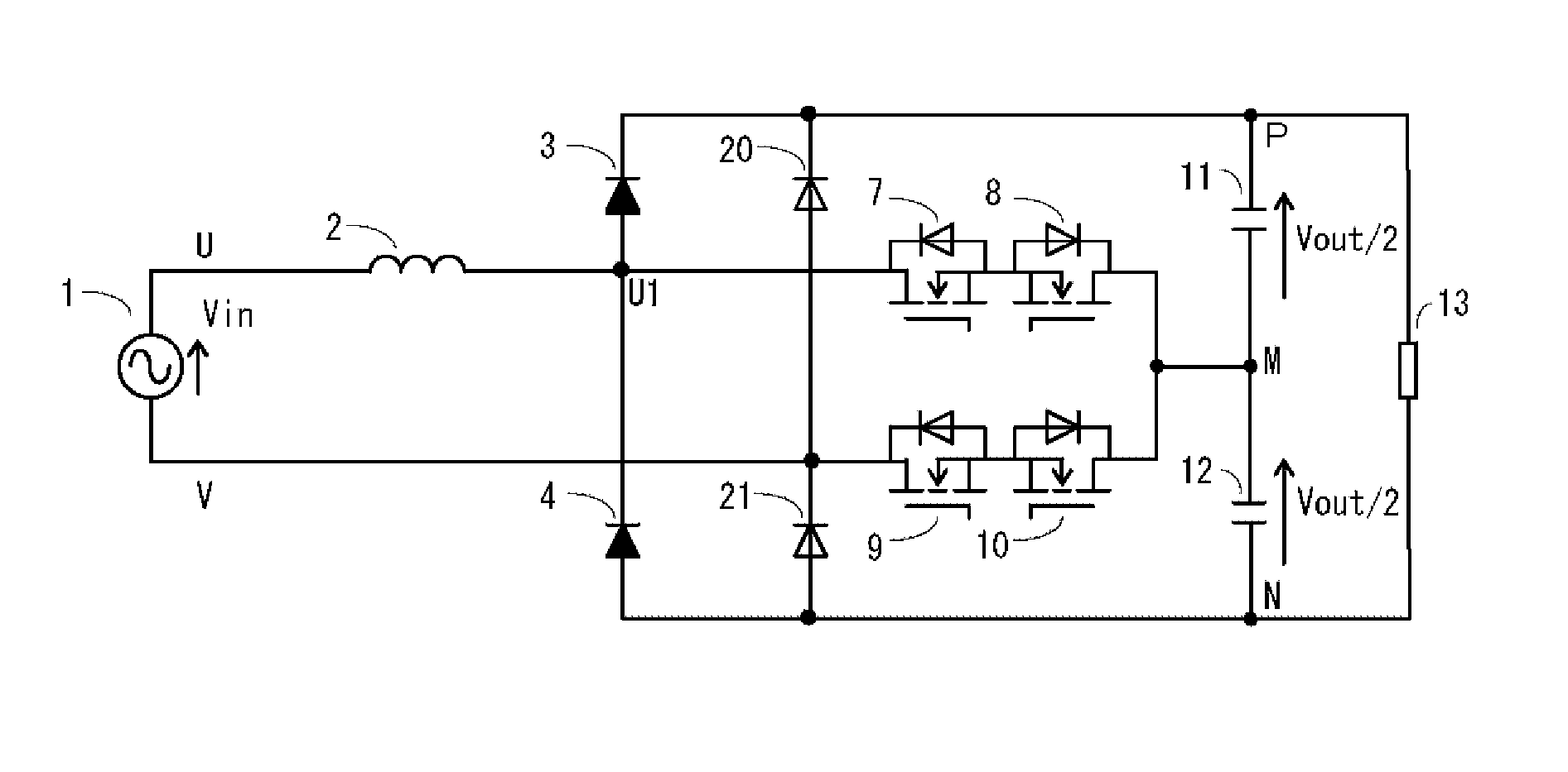
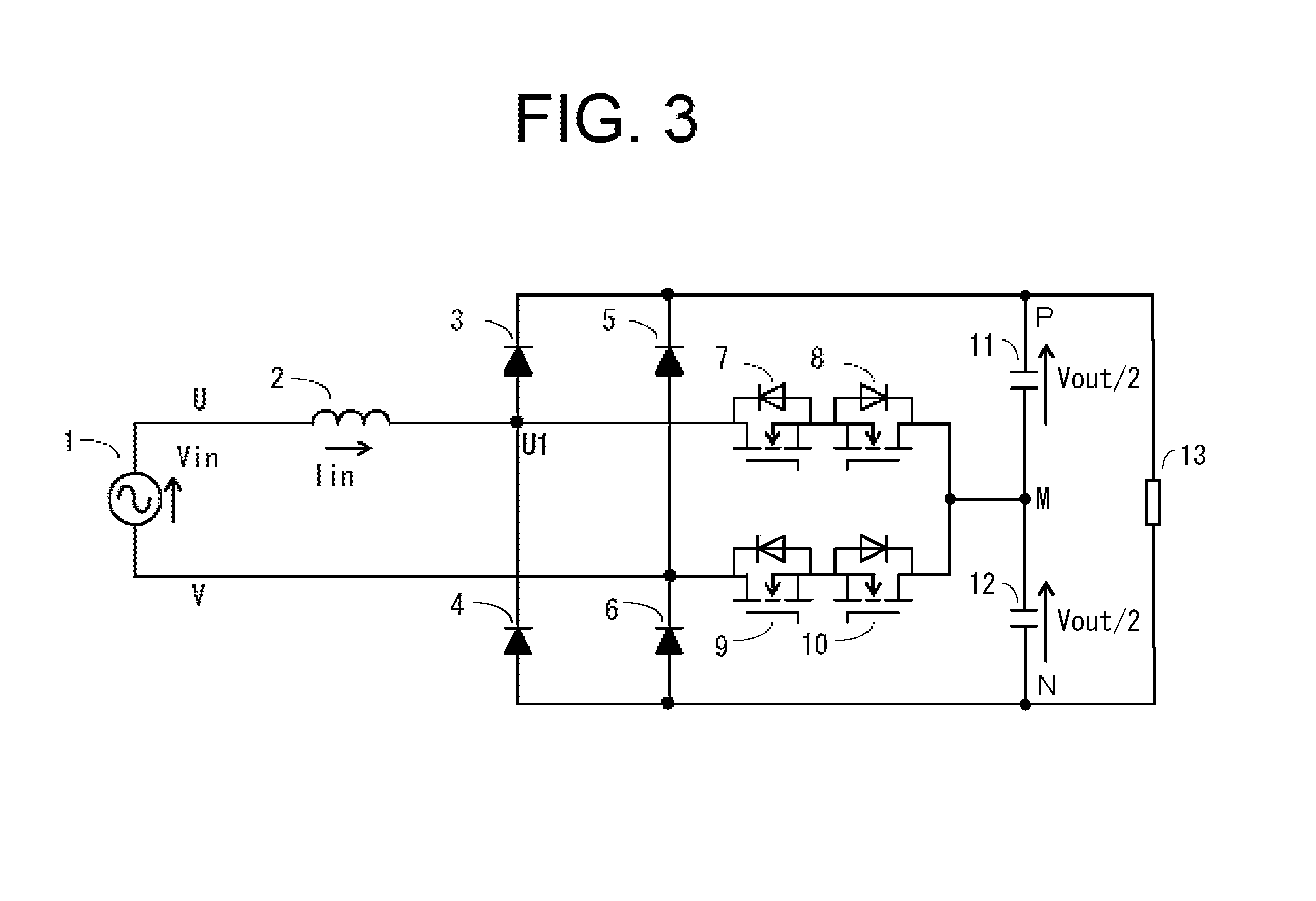
[0031]FIG. 1 shows a first embodiment of the present invention. The circuit configuration is similar to the prior art shown in FIG. 3, but the fast recovery diodes 5 and 6 in the prior art are substituted with general rectifying diodes 20 and 21. This operation is indicated below. Under conditions where the AC input voltage Vin is positive and the voltage relationship is Vin9 and 10 constituting the bi-directional semiconductor switches are kept in an on signal state at all times, and high-frequency switching is performed by the MOSFETs 7 and 8 which constitute the bi-directional semiconductor switches. In other words, the 0 voltage mode and the ½ voltage mode 1a described in the prior art example are used. The diodes 20 and 21 do not pass current in either mode. Here, the ½ voltage mode 2a is not used.
[0032]Under conditions where the AC input voltage Vin is positive and the voltage relationship is Vin>Vout / 2, the gates of the MOSFETs 9 and 10 are kept in an off signal state at all ...
second embodiment
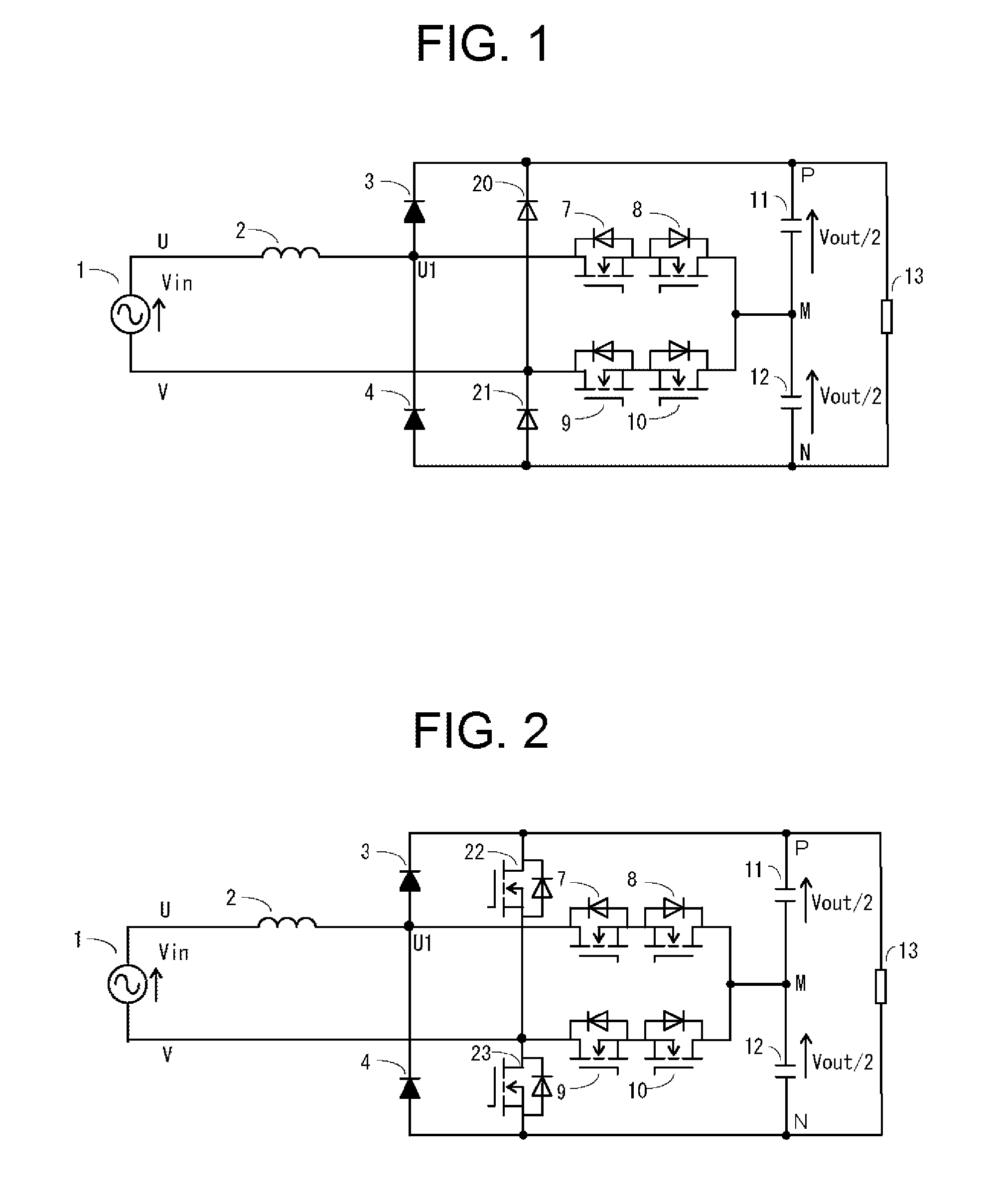
[0035]FIG. 2 shows a second embodiment of the present invention. The diodes 20 and 21 in the first embodiment are substituted with MOSFETs 22 and 23. As described above, the MOSFETs also pass current in the reverse direction by applying a voltage to the gate, and the forward voltage drop can be made small in particular when the current is small. This can be achieved by applying an on signal to one of the gates of the MOSFETs 22 and 23 in accordance with the polarity of the input current Iin, when applying an off signal to the gates of the MOSFETs 9 and 10. In recent years, the energy efficiency of power conversion devices throughout the whole period of operation has come under focus, rather than just the power conversion efficiency at the rated point. For example, with power supply devices for information equipment, or the like, it is considerably rare for the device to bear a load close to the rated power. This is because the devices are designed with spare capacity in order to pre...
third embodiment
[0037]The third embodiment uses SiC (silicon carbide) Schottky barrier diodes, instead of the fast recovery diodes according to the first and second embodiments. Since the SiC (silicon carbide) Schottky recovery diodes do not perform a reverse recovery operation, then the switching loss can be reduced yet further compared to the first and second embodiments, and the conversion efficiency of the device can be improved.
[0038]In the embodiments described above, a configuration is described in which MOSFETs are connected in reverse parallel arrangement as the bi-directional semiconductor switches, but the type of semiconductor is not limited to a MOSFET, and it is also possible to adopt a configuration in which reverse-blocking switching elements are connected in reverse parallel arrangement, or a configuration in which diodes and switching elements are combined, or the like.
PUM
 Abstract
Description
Claims
Application Information