Method for producing vapor deposition mask, and method for producing organic semiconductor element

a technology of organic semiconductor elements and vapor deposition masks, which is applied in the direction of photomechanical equipment, photosensitive material processing, instruments, etc., can solve the problems of easy distortion of slits, slit lengths, and obstacles to enhancement or upsizing of products, so as to improve definition and reduce weight , the effect of high yield

Active Publication Date: 2014-12-25
DAI NIPPON PRINTING CO LTD
View PDF8 Cites 55 Cited by
  • Summary
  • Abstract
  • Description
  • Claims
  • Application Information

AI Technical Summary

Benefits of technology

[0012]According to the method for producing a vapor deposition mask of the present invention, the vapor deposition mask capable of satisfying both enhancement in definition and reduction in weight even when a size is increased can be produced with high yield. Further, according to the method for producing an organic semiconductor element of the present invention, an organic semiconductor element can be produced with high precision.

Problems solved by technology

While in the case of using the vapor deposition mask, the vapor deposition mask is placed on a substrate front surface that should be subjected to vapor deposition and is held by using a magnet from a back surface, the rigidity of the slits is extremely small, and therefore, distortion easily occurs to the slits when the vapor deposition mask is held on the substrate front surface, which becomes an obstacle to enhancement in definition or upsizing of the products in which the slit lengths are large.
However, with the present metal processing technique, it is difficult to form slits in a large metal plate with high precision, and even if distortion in slit portions can be prevented by the method proposed in the above described Patent Literature 1 or the like, the method or the like cannot respond to enhancement in definition of the slits.
Further, in the case of use of a vapor deposition mask composed of only a metal, the mass thereof also increases with upsizing, and the total mass including a frame also increases, which becomes a hindrance to handling.

Method used


Image

  • Method for producing vapor deposition mask, and method for producing organic semiconductor element
  • Method for producing vapor deposition mask, and method for producing organic semiconductor element
  • Method for producing vapor deposition mask, and method for producing organic semiconductor element

Examples


Embodiment Construction

[0021]Hereinafter, a method for producing a vapor deposition mask of the present invention will be specifically described with use of the drawings. Note that in the following explanation, process steps will be mainly described first, and description of a material and the like will be made together when the vapor deposition mask that is produced according to the production method is described.

[0022](First Production Method)

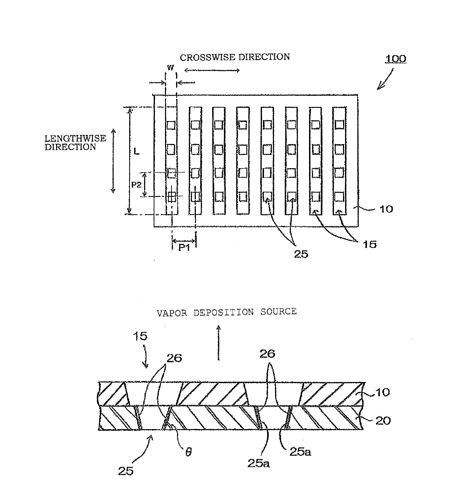
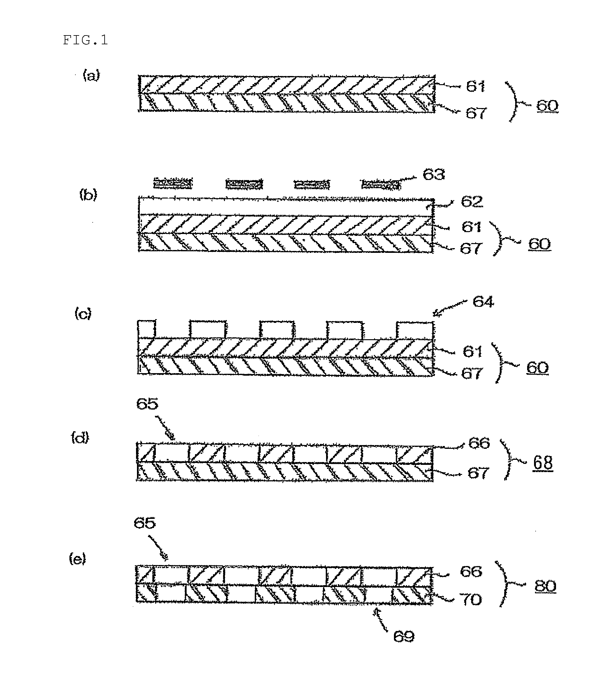
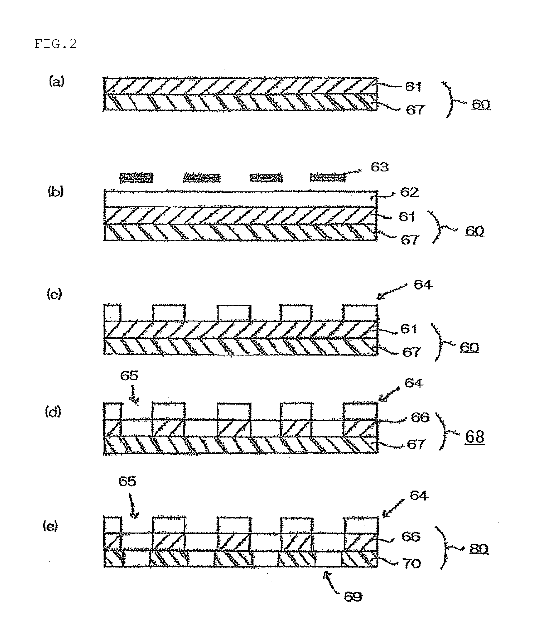
[0023]FIG. 1 is a process chart for describing a first production method of the vapor deposition mask of the present invention. Note that (a) to (e) are all sectional views.

[0024]As shown in FIG. 1 (a), a metal plate 60 with a resin layer in which a resin layer 67 is provided on one surface of the metal plate 61 is prepared. Here, a method for preparing the metal plate 60 with a resin layer is not specially limited, and the metal plate 60 with a resin layer that is commercially available may be purchased, or the metal plate 60 with a resin layer may be made by prov...


PUM

PropertyMeasurementUnit
thicknessaaaaaaaaaa
humidity absorptionaaaaaaaaaa
thicknessaaaaaaaaaa

Abstract

A method for producing a vapor deposition mask capable of satisfying both enhancement in definition and reduction in weight even when a size is increased, and a method for producing an organic semiconductor element capable of producing an organic semiconductor element with high definition are provided. A vapor deposition mask is produced by the steps of preparing a metal plate with a resin layer in which a resin layer is provided on one surface of a metal plate, forming a metal mask with a resin layer by forming a slit that penetrates through only the metal plate, for the metal plate in the metal plate with a resin layer, and thereafter, forming a resin mask by forming openings corresponding to a pattern to be produced by vapor deposition in a plurality of rows lengthwise and crosswise in the resin layer by emitting a laser from the metal mask side.

Description

TECHNICAL FIELD[0001]The present invention relates to a method for producing a vapor deposition mask, and a method for producing an organic semiconductor element.BACKGROUND ART[0002]Conventionally, in production of an organic EL element, a vapor deposition mask that is composed of a metal formed by a number of microscopic slits being arranged in parallel with one another at microscopic spaces in a region that should be subjected to vapor deposition, for example, has been used in formation of an organic layer of an organic EL element or a cathode electrode. While in the case of using the vapor deposition mask, the vapor deposition mask is placed on a substrate front surface that should be subjected to vapor deposition and is held by using a magnet from a back surface, the rigidity of the slits is extremely small, and therefore, distortion easily occurs to the slits when the vapor deposition mask is held on the substrate front surface, which becomes an obstacle to enhancement in defin...

Claims


Application Information

Patent Timeline
Patent Type & Authority Applications(United States)
IPC IPC(8): H01L51/00C23F1/14C23F1/12C23C16/04C23F1/02
CPCH01L51/0011C23C16/042C23F1/14C23F1/12C23F1/02C23C14/042C23C14/24H10K71/166H10K71/00B05B12/20G03F7/2063H10K71/233H10K50/11H10K50/82H10K71/60G03F7/20G03F7/32
Inventor TAKEDA, TOSHIHIKONISHIMURA, HIROYUKIOBATA, KATSUNARI
Owner DAI NIPPON PRINTING CO LTD
Why Eureka
Try Eureka