Device layout for reducing through-silicon-via stress
- Summary
- Abstract
- Description
- Claims
- Application Information
AI Technical Summary
Benefits of technology
Problems solved by technology
Method used
Image

Examples
Embodiment Construction
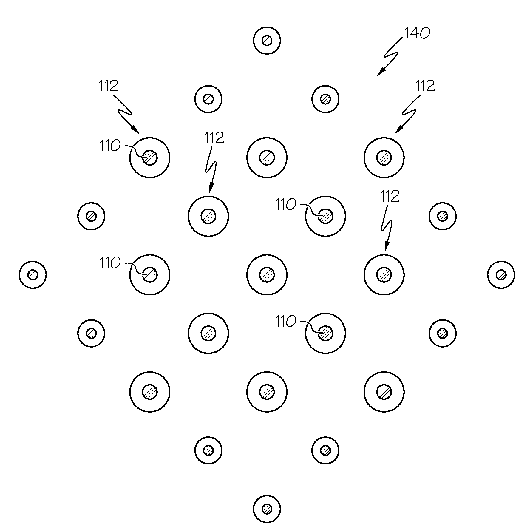
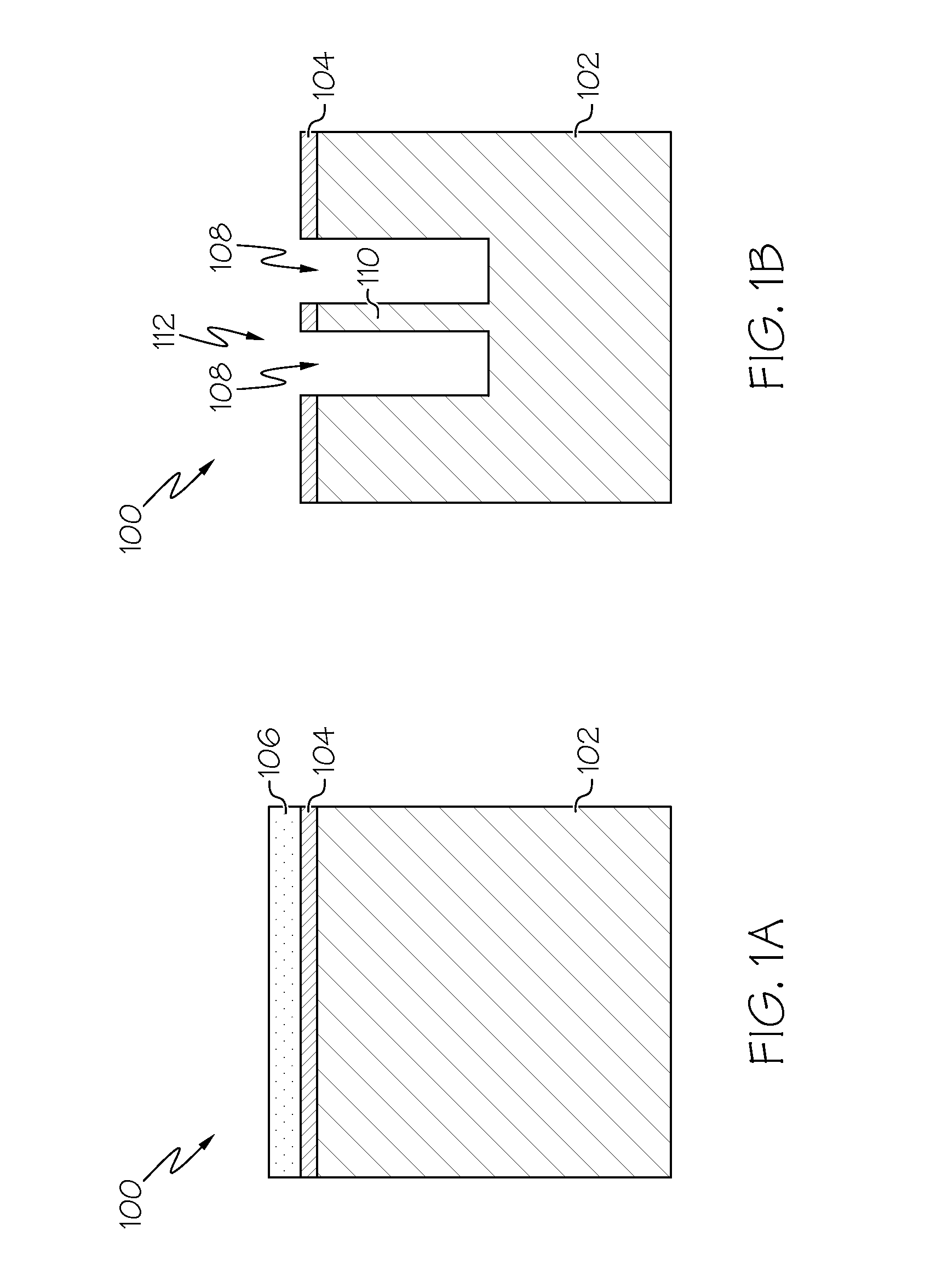
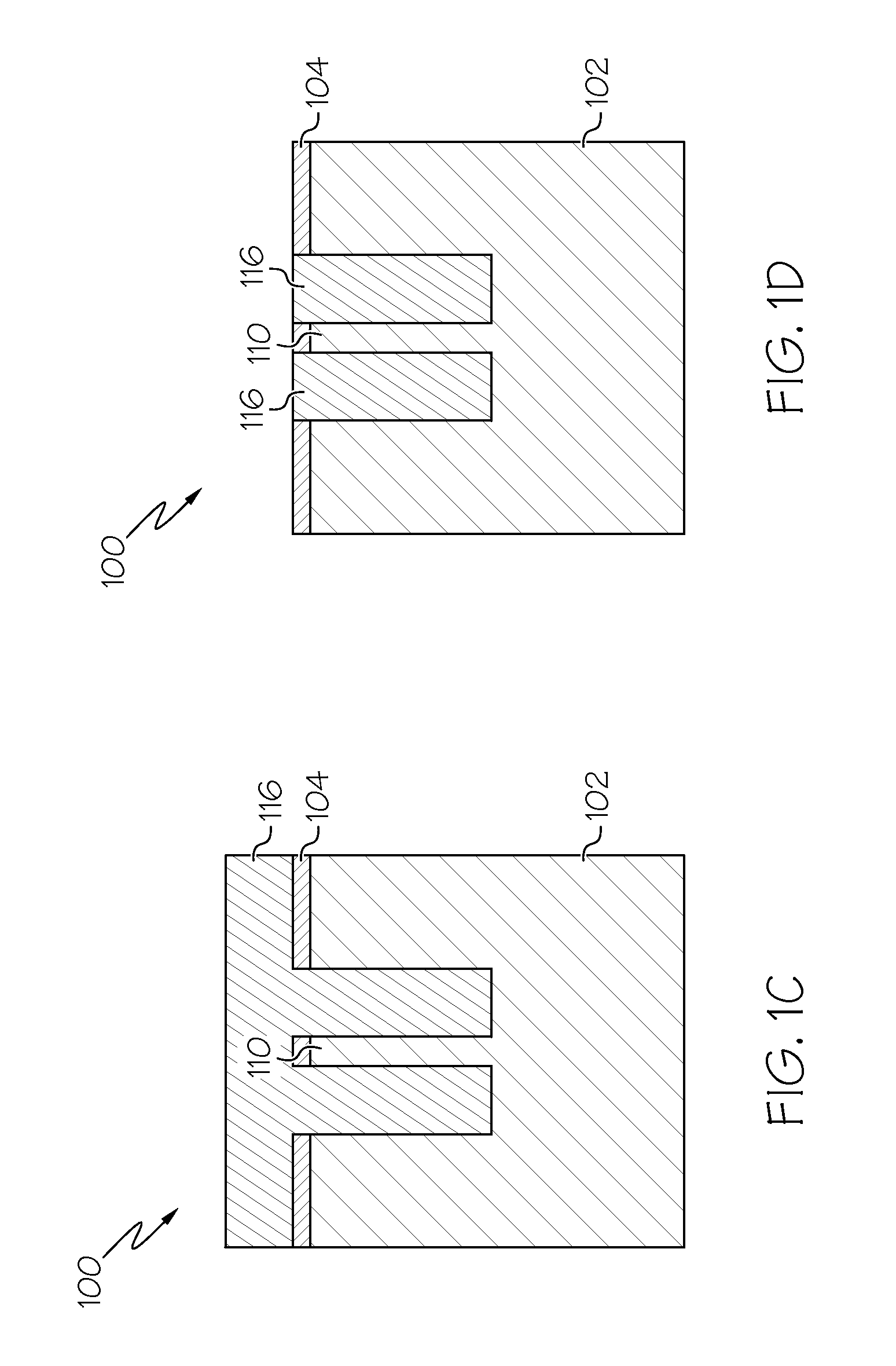
[0022]Exemplary embodiments will now be described more fully herein with reference to the accompanying drawings, in which exemplary embodiments are shown. Described are methods and techniques used for reducing through-silicon via (TSV) stress. Specifically, provided is a device comprising a substrate and a TSV formed in the substrate, the TSV having a substantially vertical element patterned therein. The TSV further comprises a set of openings adjacent the element that are subsequently filled with a TSV fill material. The element may be patterned according to any number of shapes (e.g., circle, oval, rectangle, etc.) to optimize the stress distribution for the TSV. The element is patterned and provided within the TSV in order to reduce or compensate for stress forces caused by a pronounced change in volume of the conductive fill materials of the openings of the TSV. In this manner, the high risk of creating cracks and delamination events in conventional semiconductor devices may be ...
PUM
 Abstract
Description
Claims
Application Information
 - Generate Ideas
- Intellectual Property
- Life Sciences
- Materials
- Tech Scout
- Unparalleled Data Quality
- Higher Quality Content
- 60% Fewer Hallucinations
Browse by: Latest US Patents, China's latest patents, Technical Efficacy Thesaurus, Application Domain, Technology Topic, Popular Technical Reports.
© 2025 PatSnap. All rights reserved.Legal|Privacy policy|Modern Slavery Act Transparency Statement|Sitemap|About US| Contact US: help@patsnap.com