Surface potential sensor and copying machine

a surface potential sensor and sensor technology, applied in the field of surface potential sensors and copying machines, can solve the problems of deterioration in printing quality, high manufacturing cost, and difficulty in miniaturizing the surface potential sensor, and achieve the effects of low manufacturing cost, small size of surface potential sensor, and low manufacturing cos

Active Publication Date: 2015-01-29
ORMON CORP
View PDF16 Cites 1 Cited by
  • Summary
  • Abstract
  • Description
  • Claims
  • Application Information

AI Technical Summary

Benefits of technology

[0016]The surface potential sensor according to the present invention is not required to have an actuator with a mechanical structure, a chopper mechanism or the like as in a chopper-type surface potential sensor. Hence it is possible to miniaturize the surface potential sensor and make its manufacturing cost low. Especially by mass-producing the surface potential sensor by use of the MEMS technique, it is possible to make its size very small, so as to seek for significant cost reduction. Further, in the surface potential sensor of the present invention, it is possible to enhance the measurement sensitivity by use of the electret electrode, and further to sense whether the potential of the target object is a positive potential or a negative potential. Moreover, the surface potential sensor is not required to have an actuator with a mechanical structure, a chopper mechanism or the like, but has a simple structure, and hence it is resistant to breakdown and has high reliability.

Problems solved by technology

When the charged voltage of the photosensitive drum falls below a certain level, a latent image quality deteriorates and thus less toner is applied or color unevenness occurs, leading to deterioration in printing quality.
Since a mechanical actuator is required in order to open and close the chopper, it is difficult to miniaturize the surface potential sensor.
This disables production of a MEMS (Micro Electro Mechanical Systems) device, making miniaturization of the surface potential sensor difficult and its manufacturing cost high, and also requires an operation to incorporate the component into the surface potential sensor.
With the chopper-type surface potential sensor having a large size and quite a large length as thus described, also in applications of measuring a charging potential of a photosensitive drum in a copying machine, it is impossible to ensure a space inside the copying machine which is large enough for moving the surface potential sensor along a width direction of the photosensitive drum.
Further, moving the surface potential sensor is not possible since the actuator for driving the chopper would be affected.
For that reason, this surface potential sensor can only monitor a portion of an outer periphery of the photosensitive drum, and thus has low reliability in terms of sensing deterioration in the photosensitive drum.
For this reason, when the beam portion has high rigidity, displacement in movable electrode plate is small, and it is thus difficult to obtain high measurement sensitivity.
Further, when the beam portion has low rigidity and displacement in movable electrode plate is large, inclination of the movable electrode plate becomes large at the time of displacement.
This may cause a characteristic change of the surface potential sensor depending on its installed direction, and hence it is difficult to incorporate the surface potential sensor into equipment.
Moreover, since the surface potential sensor is greatly affected by acceleration due to vibration, it is also difficult to perform accurate measurement.
Furthermore, in such a surface potential sensor, the movable electrode plate is attracted to the charged object regardless of the polarity (positive or negative voltage) of the charged object, and hence it is not possible to find the polarity of the charged object.

Method used


Image

  • Surface potential sensor and copying machine
  • Surface potential sensor and copying machine
  • Surface potential sensor and copying machine

Examples


first embodiment

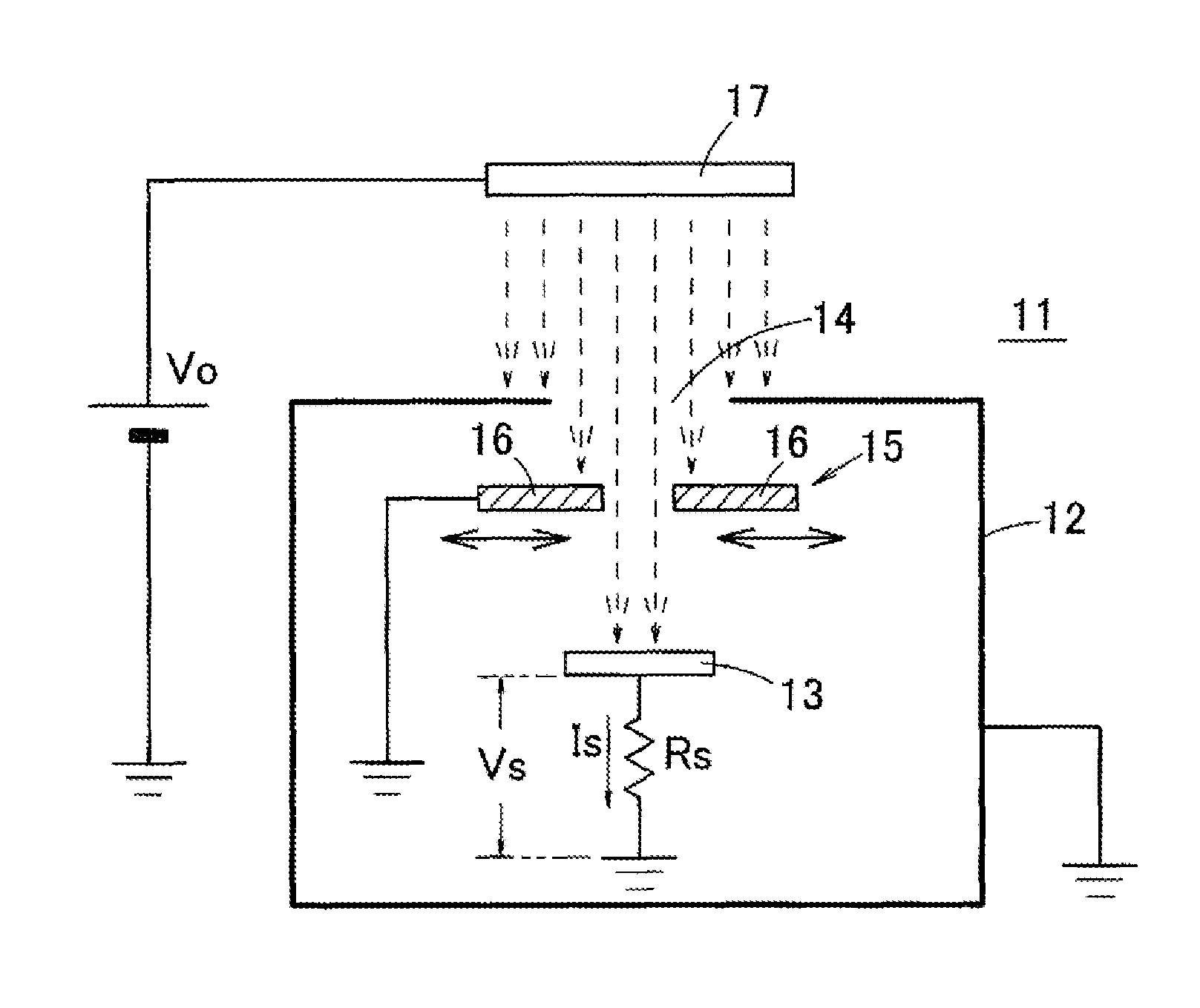
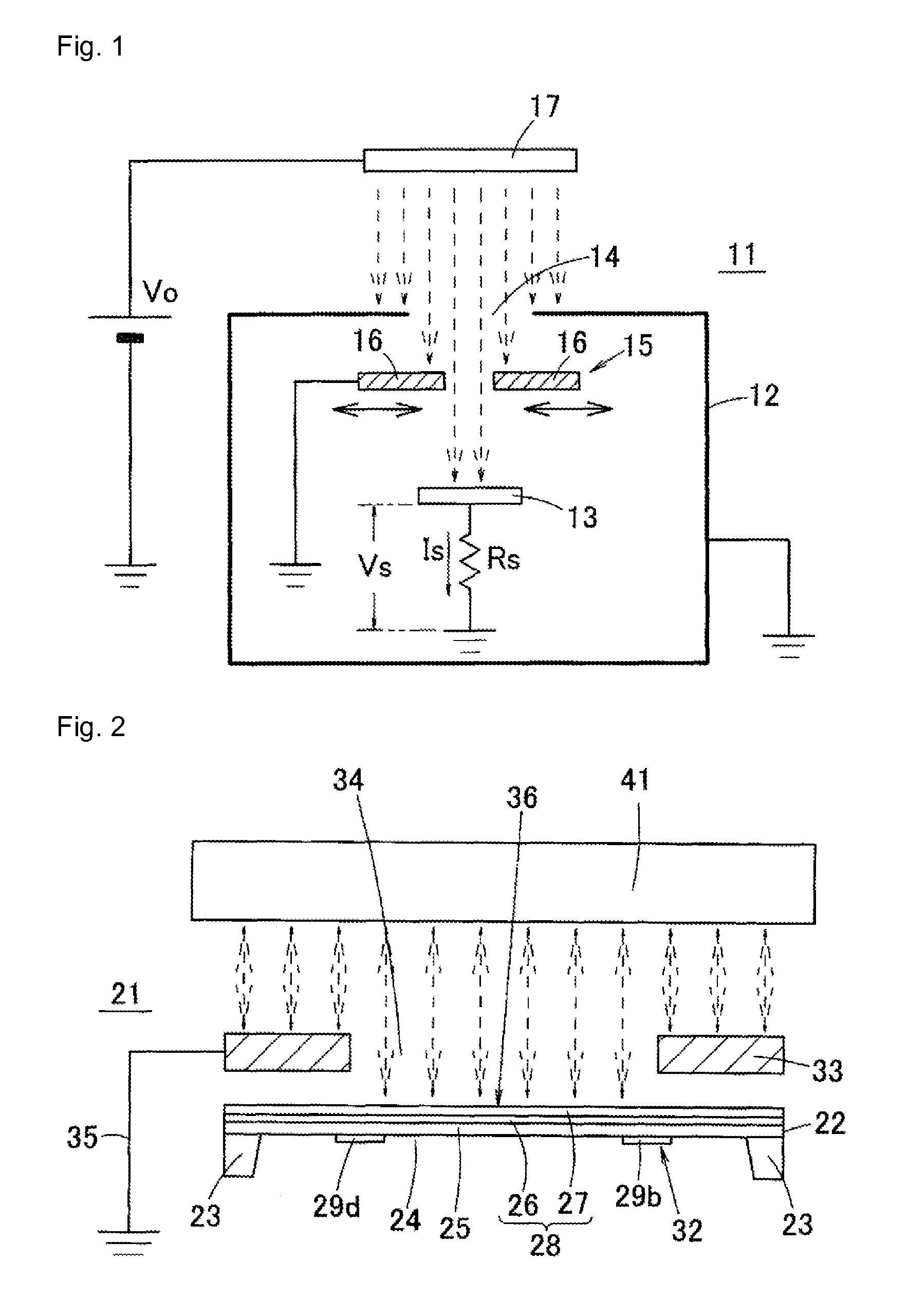
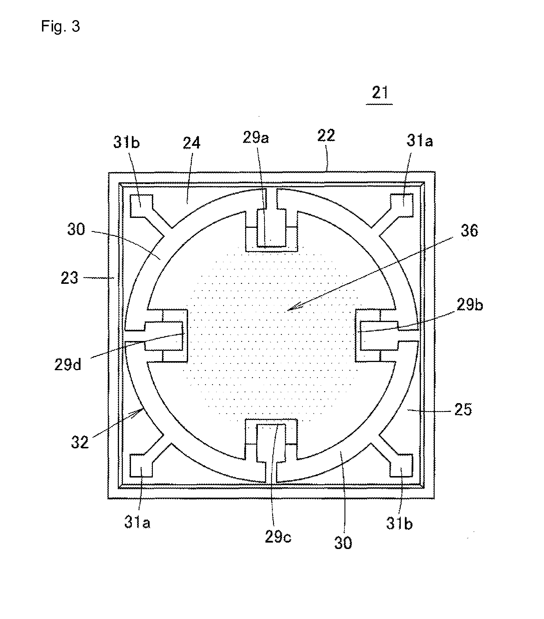
[0029]Hereinafter, a surface potential sensor 21 according to the first embodiment of the present invention will be described with reference to FIGS. 2, 3 and 4. FIG. 2 is a schematic sectional view of a surface potential sensor 21 according to the first embodiment of the present invention, FIG. 3 is a bottom view of a surface potential sensor 21, and FIG. 4 is a circuit diagram showing a distortion quantity detecting unit 32 in the surface potential sensor 21.

[0030]As shown in FIG. 2, a support 23 with a relatively large thickness is provided on an outer peripheral portion of the lower surface of a semiconductor substrate 22 such as a silicon substrate, and a recessed portion 24 surrounded by the support 23 is formed on the lower surface of the semiconductor substrate 22. A thin-film diaphragm 25 (semiconductor layer) located on the recessed portion 24 is floating in a space through support by the support 23. A metal film 26 is formed on the upper surface of the semiconductor subst...

second embodiment

[0064]FIG. 5 is a schematic sectional view showing a surface potential sensor 45 according to a second embodiment of the present invention. In this surface potential sensor 45, a recessed portion 24 is formed by etching on the lower surface of a semiconductor substrate 22 such as a silicon substrate, and a support 23 is formed therearound. Further, a thin-film diaphragm 25 is formed of the semiconductor substrate 22 on the recessed portion 24, and piezoresistors 29a to 29d are provided on the upper surface of the diaphragm 25. Moreover, the upper surface of the semiconductor substrate 22 is covered by an insulating layer 38 such as an oxide film or a nitride film, on which an electret electrode 28 made up of a metal film 26 and an electret film 27 is formed.

[0065]In this surface potential sensor 45, piezoresistors 29a to 29d are produced on the upper surface of semiconductor substrate 22 (wafer), and further, the insulating layer 38, the metal film 26 and the electret film 27 are se...

third embodiment

[0066]FIG. 6 is a schematic sectional view of surface potential sensor 51 according to a third embodiment of the present invention. In this surface potential sensor 51, a base 53 is provided on the upper surface of a tabular substrate 52, and a sensing lever 54 (deformable member) is provided on the base 53. The sensing lever 54 has a base portion fixed to the upper surface of the base 53, and a leading end portion curved upward and extended away from the base 53. Further, a strain gauge 55 (distortion quantity detecting device) is fitted to a portion where the largest distortion occurs when force is applied to the sensing lever 54. This sensing lever 54 and the strain gauge 55 constitute an electrostatic force detector. Further, on the upper surface of the substrate 52, an elastic material 56 such as silicon rubber is molded so as to embed the base 53, the sensing lever 54 and the strain gauge 55. The upper surface of the elastic material 56 is formed flat, and the electret electro...


PUM


Abstract

This surface potential sensor is provided with an electret electrode (28), which is configured of a metal film (26) and an electret film (27), said electret electrode being provided on an upper surface of a diaphragm (25) of a semiconductor substrate. Four piezoresistors (29a, 29b, 29c, 29d) are formed on the diaphragm (25), and a distortion quantity detecting unit (32) is configured by forming a bridge circuit using the piezoresistors. Since an electrostatic force that operates between an object and the electret electrode (28) changes corresponding to potential of the object, and the electret electrode (28) warps corresponding to the change, the potential of the object can be detected by measuring a distortion quantity of the electret electrode (28) by means of the distortion quantity detecting unit (32). Consequently, not only the potential of the object but also a polarity thereof can be detected with reduced size and high sensitivity.

Description

TECHNICAL FIELD[0001]The present invention relates to a surface potential sensor and a copying machine. The present invention specifically relates to a surface potential sensor for measuring a surface potential of a target object by use of electrostatic force that operates between itself and the target object, and a copying machine provided with the surface potential sensor.BACKGROUND ART[0002]In a variety of equipment such as a copying machine, a printer and a liquid crystal display device, a surface potential of a specific portion in the equipment is measured. For example, as a photosensitive drum is used repeatedly in an electrostatic copying machine, a charged voltage of the photosensitive drum gradually decreases. When the charged voltage of the photosensitive drum falls below a certain level, a latent image quality deteriorates and thus less toner is applied or color unevenness occurs, leading to deterioration in printing quality. Therefore, a charged voltage of the photosensi...

Claims


Application Information

Patent Timeline
Patent Type & Authority Applications(United States)
IPC IPC(8): G01R29/12
CPCG01R29/12G01R5/28G01R15/14G01R15/165G01R19/0023G01R29/08G01R29/0814G01R29/0842G01R31/2642G03G15/5037
Inventor MATSUSHITA, SOICHI
Owner ORMON CORP
Why Eureka
Try Eureka