Combined X-Ray and Optical Metrology

a technology of optical metrology and x-ray, applied in the field of metalrology systems and methods, can solve the problems of difficult optical radiation penetration to the bottom layer, difficult characterization, and increased difficulty in characterization, so as to reduce the number of floating target parameters of the optical model and the number of floating target parameters of the x-ray model

Active Publication Date: 2015-01-29
KLA TENCOR TECH CORP
View PDF6 Cites 48 Cited by
  • Summary
  • Abstract
  • Description
  • Claims
  • Application Information

AI Technical Summary

Benefits of technology

[0013]In yet another further aspect, the number of floating target parameters of the optical model and the number of floating target parameters of the x-ray model are reduced by linking some of the parameters. In some examples, common geometric parameters are treated as a single parameter. In some other examples, it may be necessary to introduce scaling factors and offset values to account for calibration and model bias associated with different metrologies.

Problems solved by technology

As devices (e.g., logic and memory devices) move toward smaller nanometer-scale dimensions, characterization becomes more difficult.
Devices incorporating complex three-dimensional geometry and materials with diverse physical properties contribute to characterization difficulty.
For example, modern memory structures are often high-aspect ratio, three-dimensional structures that make it difficult for optical radiation to penetrate to the bottom layers.
As a result, the parameters characterizing the target often cannot be reliably decoupled with available measurements.
Optical radiation is often unable to penetrate layers constructed of these materials.
As a result, measurements with thin-film scatterometry tools such as ellipsometers or reflectometers are becoming increasingly challenging.
In response to these challenges, more complex optical tools have been developed.
However, these approaches have not reliably overcome fundamental challenges associated with measurement of many advanced targets (e.g., complex 3D structures, structures smaller than 10 nm, structures employing opaque materials) and measurement applications (e.g., line edge roughness and line width roughness measurements).
Future metrology applications present challenges for metrology due to increasingly small resolution requirements, multi-parameter correlation, increasingly complex geometric structures, and increasing use of opaque materials.

Method used


Image

  • Combined X-Ray and Optical Metrology
  • Combined X-Ray and Optical Metrology
  • Combined X-Ray and Optical Metrology

Examples


Embodiment Construction

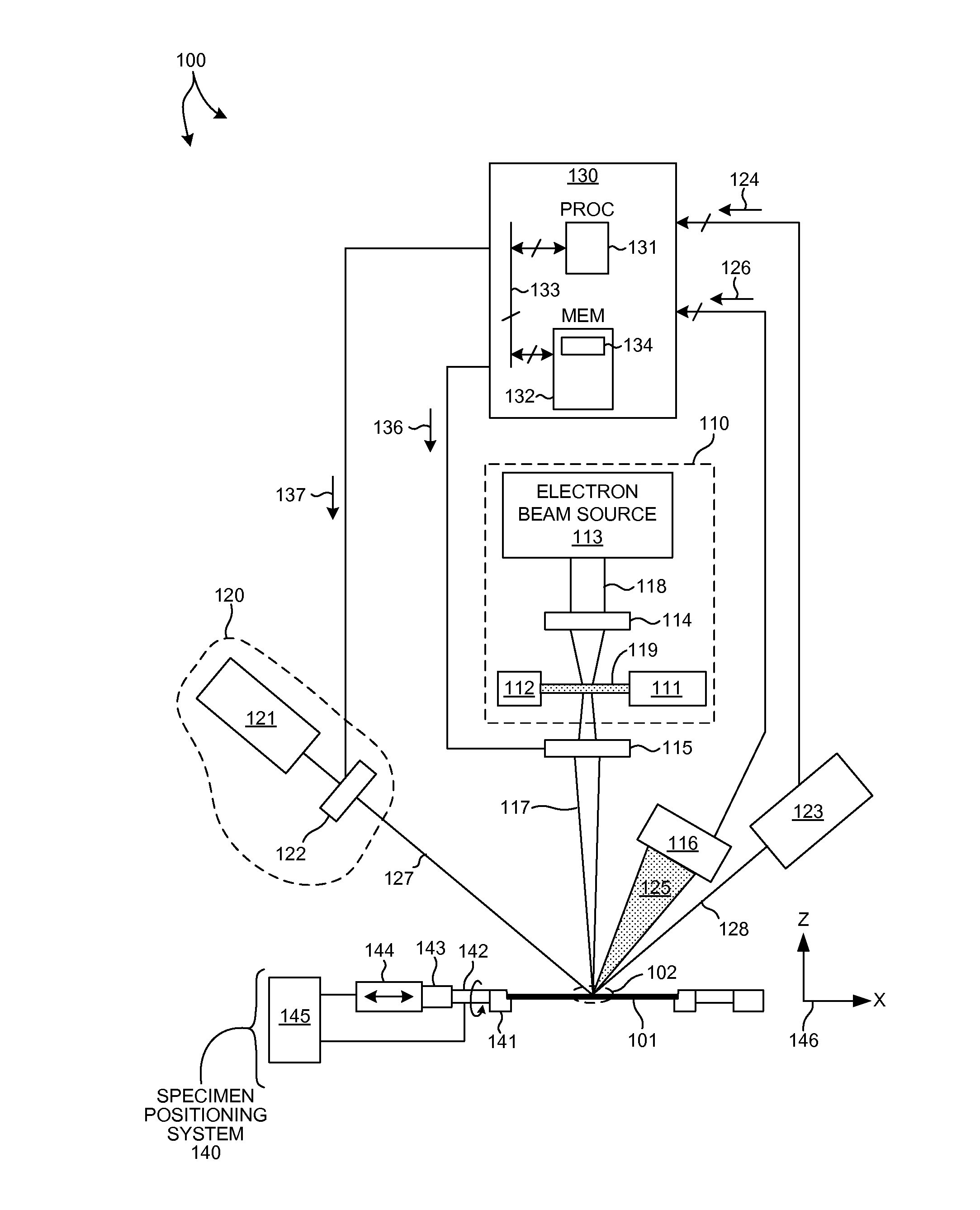
[0023]Methods and systems for performing measurements of structural and material characteristics (e.g., material composition, dimensional characteristics of structures and films, etc.) associated with different semiconductor fabrication processes are presented. As described herein, one or more structural parameters of a semiconductor specimen are determined by fitting models of the response of the specimen to measurements collected by different measurement techniques in a combined analysis. Reference will now be made in detail to background examples and some embodiments of the invention, examples of which are illustrated in the accompanying drawings.

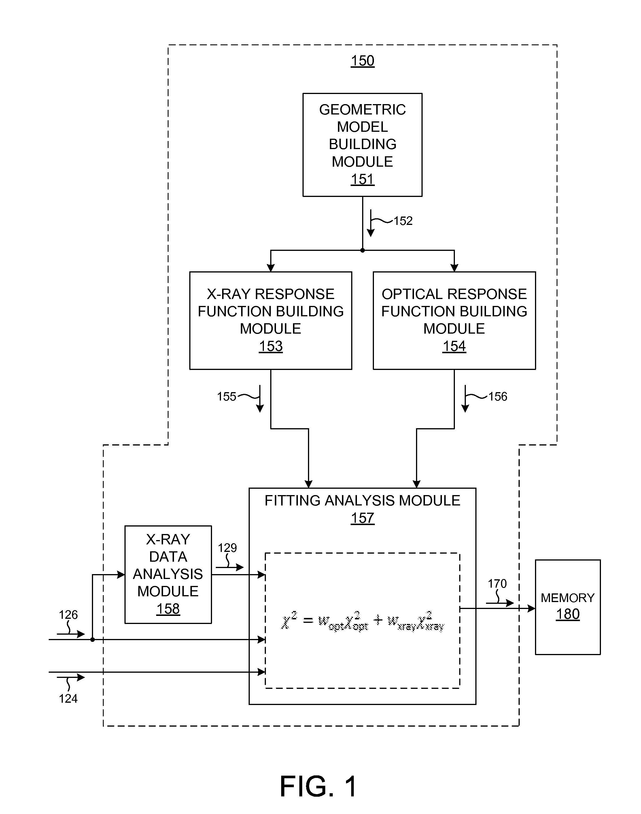
[0024]In one aspect, x-ray measurement data of a specimen is analyzed to determine at least one specimen parameter value that is treated as a constant in a combined analysis of both optical measurements and x-ray measurements of the specimen. For example, a particular structural property (e.g., layer thickness, structure volume, etc.), o...


PUM

PropertyMeasurementUnit
roughnessaaaaaaaaaa
optical responseaaaaaaaaaa
opticalaaaaaaaaaa

Abstract

Structural parameters of a specimen are determined by fitting models of the response of the specimen to measurements collected by different measurement techniques in a combined analysis. X-ray measurement data of a specimen is analyzed to determine at least one specimen parameter value that is treated as a constant in a combined analysis of both optical measurements and x-ray measurements of the specimen. For example, a particular structural property or a particular material property, such as an elemental composition of the specimen, is determined based on x-ray measurement data. The parameter(s) determined from the x-ray measurement data are treated as constants in a subsequent, combined analysis of both optical measurements and x-ray measurements of the specimen. In a further aspect, the structure of the response models is altered based on the quality of the fit between the models and the corresponding measurement data.

Description

CROSS REFERENCE TO RELATED APPLICATION[0001]The present application for patent claims priority under 35 U.S.C. §119 from U.S. provisional patent application Ser. No. 61 / 867,363, entitled “Method of Measuring Semiconductor Structure Parameters Using Optical and X-Ray Absorbance-Emission Metrology Technologies,” filed Aug. 19, 2013, the subject matter of which is incorporated herein by reference in its entirety.TECHNICAL FIELD[0002]The described embodiments relate to metrology systems and methods, and more particularly to methods and systems for improved measurement accuracy.BACKGROUND INFORMATION[0003]Semiconductor devices such as logic and memory devices are typically fabricated by a sequence of processing steps applied to a specimen. The various features and multiple structural levels of the semiconductor devices are formed by these processing steps. For example, lithography among others is one semiconductor fabrication process that involves generating a pattern on a semiconductor ...

Claims


Application Information

Patent Timeline
Patent Type & Authority Applications(United States)
IPC IPC(8): G01N23/203G01B15/00
CPCG01B15/00G01N23/203G01B2210/56H01L22/12H01L22/20G01N23/2206
Inventor PETERLINZ, KEVIN A.SHCHEGROV, ANDREI V.BAKEMAN, MICHAEL S.DZIURA, THADDEUS GERARD
Owner KLA TENCOR TECH CORP
Why Eureka
Try Eureka