

Inductor
a technology of inductor and integrated circuit, which is applied in the direction of transformer/inductance coil/winding/connection, multiple-port active network, etc., can solve the problems of large size of semiconductor integrated circuit and rise in cost of semiconductor integrated circuit, and achieves large band extension effect, high speed, and low cost of providing semiconductor integrated circui
- Summary
- Abstract
- Description
- Claims
- Application Information
AI Technical Summary
Benefits of technology
Problems solved by technology
Method used
Image

Examples
first embodiment
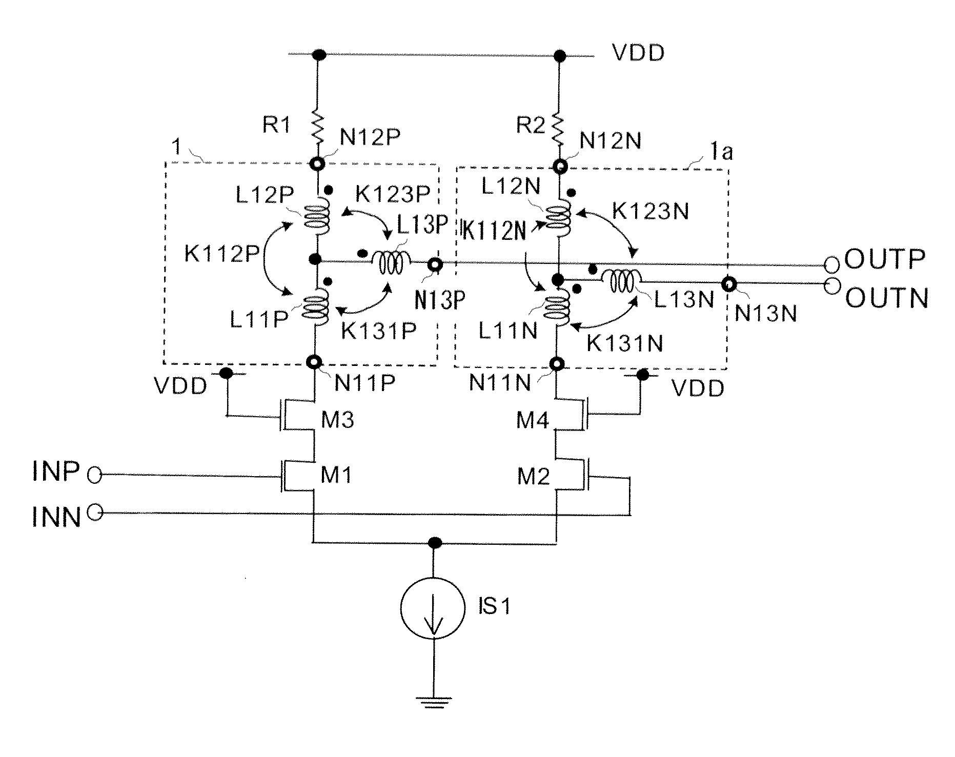
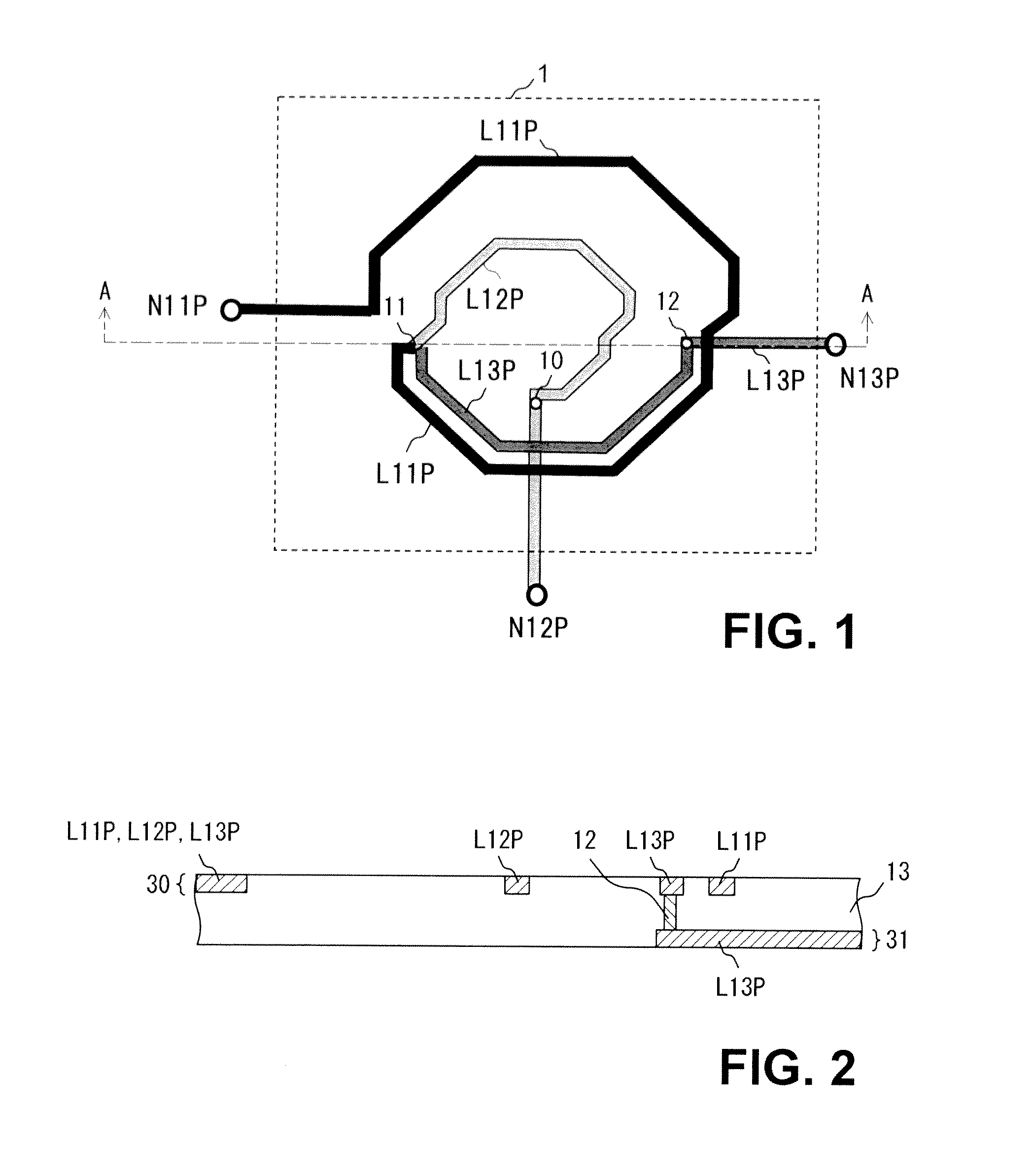
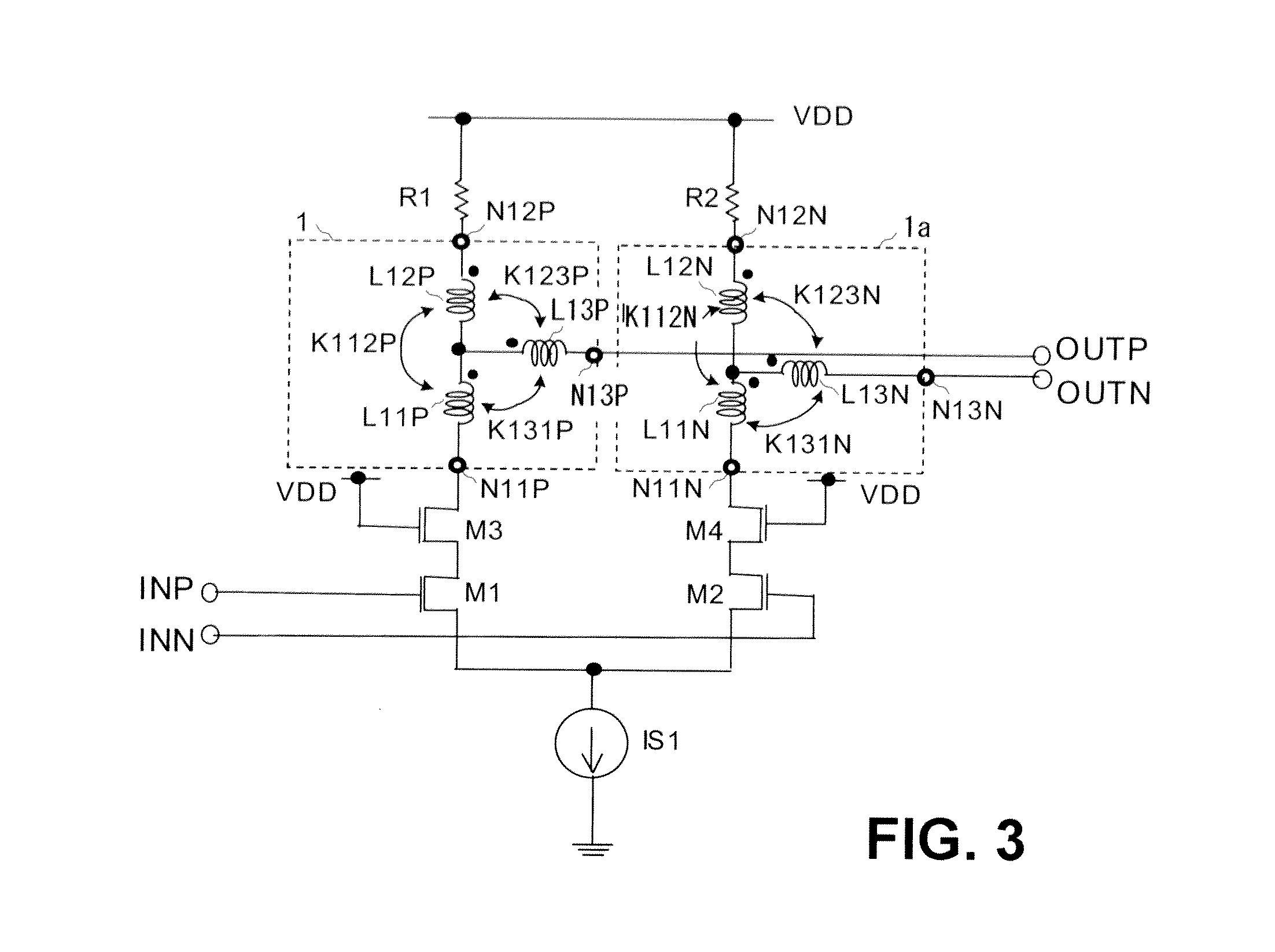
[0026]An embodiment of the present invention will now be described with reference to the accompanying drawings. FIG. 1 is a plan view of an inductor according to the first embodiment of the present invention. FIG. 2 is a sectional view of the inductor taken along a line A-A in FIG. 1. Note that FIG. 1 perspectively illustrates a plurality of metal wiring layers. Referring to FIG. 1, an inductor 1 according to this embodiment includes a first shunt inductor L11P (first inductor wire), a second shunt inductor L12P (second inductor wire), and a first series inductor L13P (third inductor wire).
[0027]The rectangular or circular region where the inductors L11P, L12P, and L13P are formed will be referred to as an inductor region hereinafter. In the example shown in FIG. 1, a region indicated by the dotted line is the inductor region.
[0028]The first shunt inductor L11P is formed using a first metal wiring layer 30. The first shunt inductor L11P is formed into a spiral that makes a round on ...
second embodiment
[0050]The second embodiment will be described next. FIG. 4 is a plan view of an inductor according to the second embodiment of the present invention. FIG. 5 is a sectional view of the inductor taken along a line B-B in FIG. 4. Note that FIG. 4 perspectively illustrates a plurality of metal wiring layers. In this embodiment, three inductors used on the positive-phase side of a differential circuit and three inductors used on the negative-phase side are wound into one spiral. Referring to FIG. 4, an inductor 2 according to this embodiment includes a first shunt inductor L11P (first inductor wire) on the positive-phase side, a second shunt inductor L12P (second inductor wire) on the positive-phase side, a first series inductor L13P (third inductor wire) on the positive-phase side, a first shunt inductor L11N (fourth inductor wire) on the negative-phase side, a second shunt inductor L12N (fifth inductor wire) on the negative-phase side, and a first series inductor L13N (sixth inductor w...
PUM
 Abstract
Description
Claims
Application Information