Chip package and fabrication method thereof

a technology of chip package and fabrication method, which is applied in the direction of semiconductor devices, electrical devices, semiconductor/solid-state device details, etc., can solve the problems of increasing the reliability of the chip package, increasing increasing the complexity of the semiconductor chip. , to achieve the effect of reducing the cost of the manufacturing process and the process time, reducing one photomask, and improving production capacity

Active Publication Date: 2015-02-12
XINTEC INC
View PDF5 Cites 7 Cited by
  • Summary
  • Abstract
  • Description
  • Claims
  • Application Information

AI Technical Summary

Benefits of technology

[0016]As a result, a photolithography process and a corresponding etching process do not need to be used to remove the first insulating layer on the surface of the conductive pad, and the first insulating layer may be synchronously removed with the second insulating layer during one etching process, so as to reduce one photomask. Therefore, the cost of the manufacturing process and the process time are reduced, such that the production capacity is improved.

Problems solved by technology

As demand for electronic or optoelectronic products, such as digital cameras, camera phones, bar code readers, and monitors, increase, semiconductor technology for products made therefrom must develop rapidly, as product trends demand the semiconductor chip size to be miniaturized and functionality of the semiconductor chip to be increased and become more complex.
However, since there is mismatch of the coefficient of thermal expansion (CTE) between a passivation layer and a metal redistribution layer (RDL) in a chip package, the metal RDL easily peels off from conductive pads of the semiconductor chip, thus, reducing the reliability of the chip package.
The cost of the manufacturing process and the process time are therefore increased, which make the improvement of the production capacity even more difficult.

Method used


Image

  • Chip package and fabrication method thereof
  • Chip package and fabrication method thereof
  • Chip package and fabrication method thereof

Examples


Embodiment Construction

[0031]Reference will now be made in detail to the present embodiments of the invention, examples of which are illustrated in the accompanying drawings. Wherever possible, the same reference numbers are used in the drawings and the description to refer to the same or like parts.

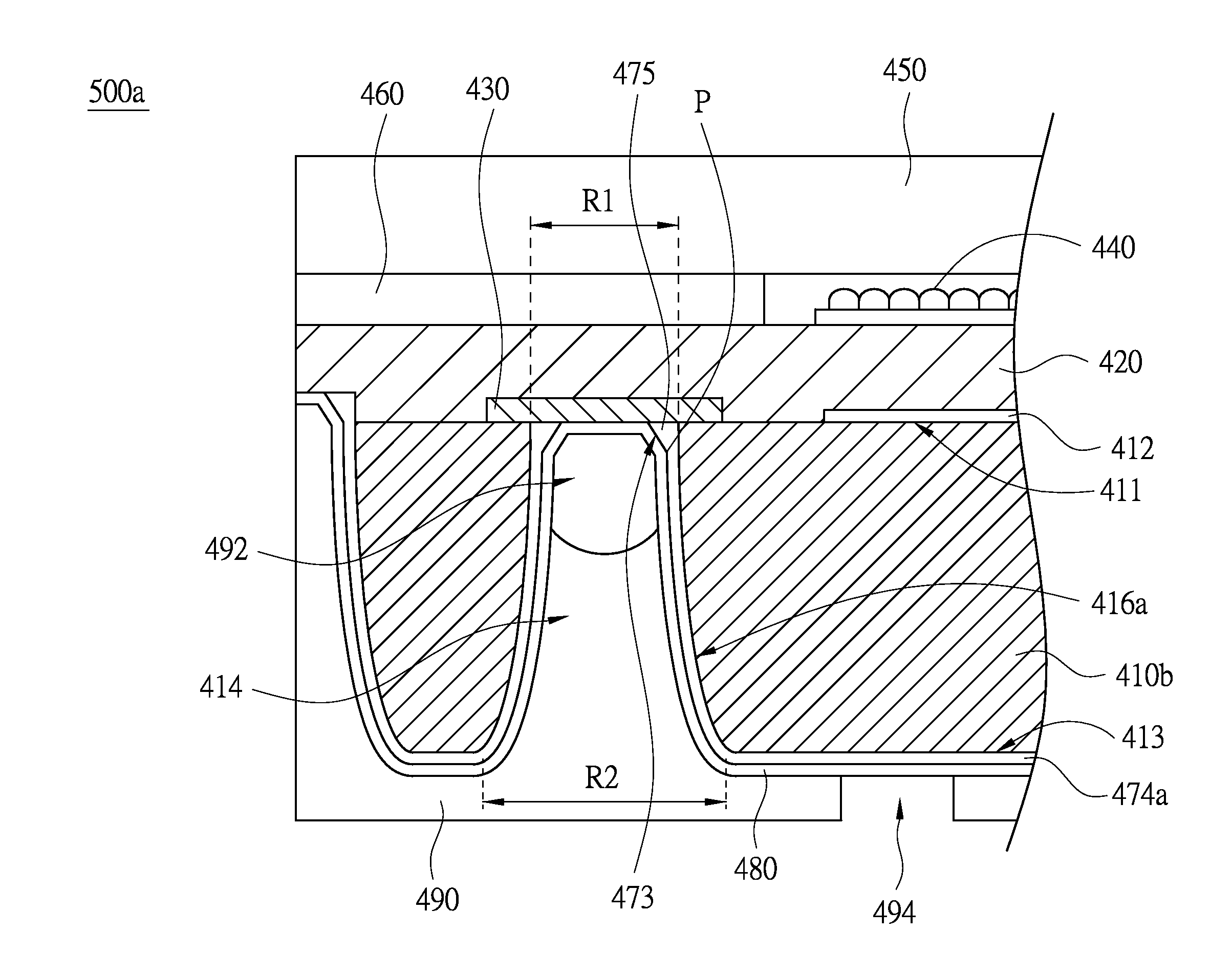
[0032]Referring to FIG. 1I, which illustrates a cross section of an exemplary embodiment of a chip package according to the invention. In the embodiment, the chip package may be applied to various electronic components including active or passive elements, digital or analog integrated circuits, such as optoelectronic devices, micro electro mechanical systems (MEMS), micro fluidic systems, and physical sensors for detecting physical characteristics such as detecting heat, light, or pressure. In particular, a wafer level package (WLP) process may be performed to package semiconductor chips which include image sensor devices, light-emitting diodes (LEDs), solar cells, RF circuits, accelerators, gyroscopes, micro ...


PUM


Abstract

A fabrication method of a chip package includes the following steps. A wafer structure having a wafer and a protection layer is provided. The first opening of the wafer is aligned with and communicated with the second opening of the protection layer. A first insulating layer having a first thickness is formed on a conductive pad exposed from the second opening, and a second insulating layer having a second thickness is formed on a first sidewall of the protection layer surrounding the second opening and a second sidewall of the wafer surrounding the first opening. The first and second insulating layers are etched, such that the first insulating layer is completely removed, and the second thickness of the second insulating layer is reduced.

Description

RELATED APPLICATIONS[0001]This application is a Continuation-In-Part of pending U.S. patent application Ser. No. 13 / 369,085, filed Feb. 8, 2012, which claims the benefit of U.S. Provisional Application No. 61 / 441,507, filed Feb. 10, 2011. This application also claims the benefit of U.S. Provisional Application No. 61 / 868,312, filed Aug. 21, 2013. The entirety of which are incorporated by reference herein.BACKGROUND[0002]1. Field of Invention[0003]The invention relates to a chip package and more particularly to a chip package with a through substrate via (TSV) structure and a fabrication method thereof.[0004]2. Description of Related Art[0005]As demand for electronic or optoelectronic products, such as digital cameras, camera phones, bar code readers, and monitors, increase, semiconductor technology for products made therefrom must develop rapidly, as product trends demand the semiconductor chip size to be miniaturized and functionality of the semiconductor chip to be increased and b...

Claims


Application Information

Patent Timeline
Patent Type & Authority Applications(United States)
IPC IPC(8): H01L23/00H01L21/311H01L21/02
CPCH01L24/06H01L24/03H01L21/02271H01L21/31111H01L2224/05024H01L2224/0237H01L2224/0382H01L2224/0401H01L2224/05026H01L2224/0231H01L21/76898H01L23/3114H01L23/481H01L23/525H01L24/13H01L27/14618H01L27/14627H01L33/58H01L33/62H01L2224/02372H01L2224/05548H01L2224/13022H01L2224/13024H01L2924/0001H01L2924/1461H01L2924/15788H01L24/05H01L2224/02377H01L2224/05022H01L2224/05567H01L2224/94H01L27/14623H01L21/561H01L21/76831H01L2224/05599H01L2224/13099H01L2924/00H01L2224/03H01L2224/11H01L31/02005H01L31/02327H01L27/14685H01L31/1876H01L2933/0058H01L2933/0066
Inventor LIN, CHIA-SHENG
Owner XINTEC INC
Why Eureka
Try Eureka