Patterned conductive film, method of fabricating the same, and application thereof

a technology conductive film, which is applied in the field of patterned conductive film, can solve the problems of environmental pollution and visible etching marks

Active Publication Date: 2015-02-19
HANNSTAR DISPLAY CORPORATION
View PDF4 Cites 20 Cited by
  • Summary
  • Abstract
  • Description
  • Claims
  • Application Information

AI Technical Summary

Benefits of technology

[0082]In case the concept of the embodiments of the disclosure is applied to the touch panel, if a dry patterning process can be adopted, and a printing technology is used in the regulating layer and the touch sensor bridge electrode, the costs thereof can be lowered. In addition, the silver nanowire may provide high conductivity and an element structure being flexible without visible etching marks.
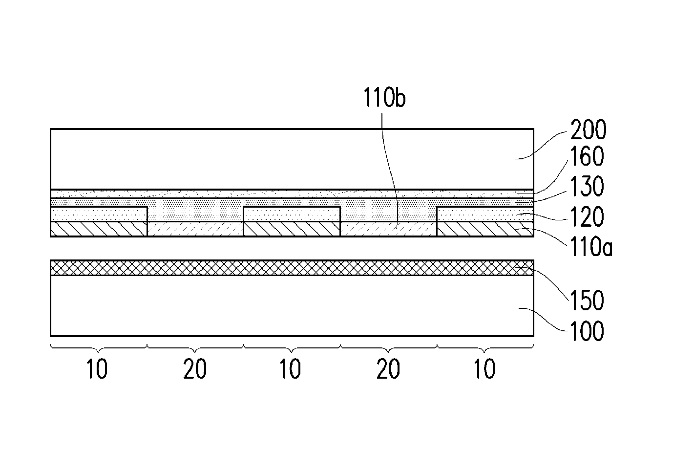
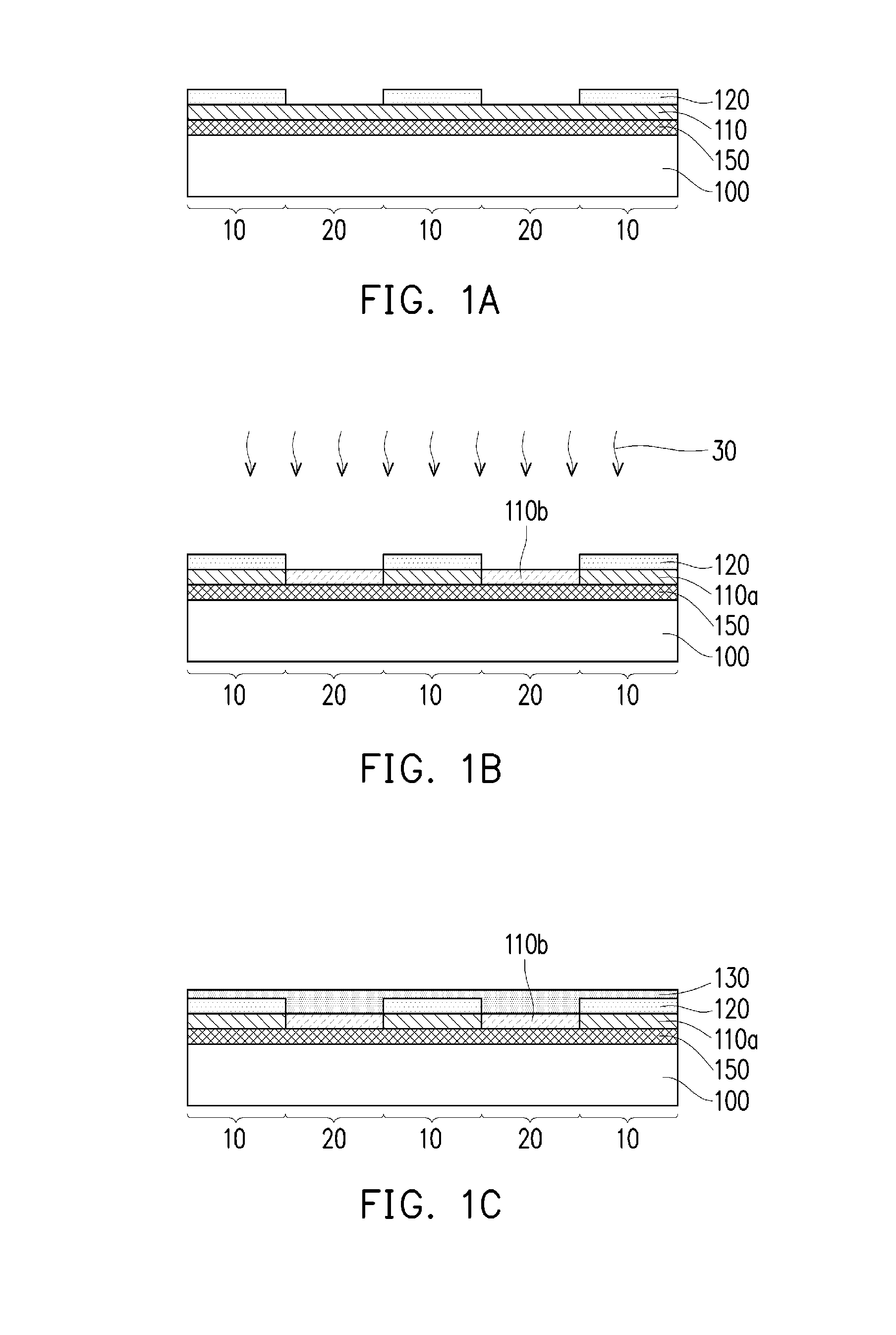
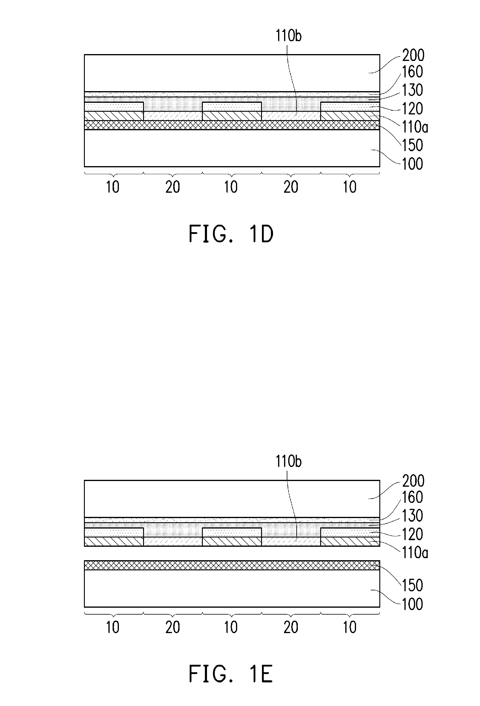
[0093]In an embodiment of the disclosure, the patterned regulating layer contacting the conductive interconnected nano-structure film together with specific conductivity regulating treatments are utilized, such that the conductive interconnected nano-structure film can provide characteristics in a regional high conductivity and a regional low conductivity, so as to accomplish the purpose of patterning the conductive interconnected nano-structure film. Also, since the interconnected nano-structure film being processed with energy is not etch-dissolved or removed. No visible etching marks are left after the conductive film is patterned, so that an optical quality thereof can be improved. The fabricating method of the patterned conductive film according to the embodiments of the disclosure can reduce uses of mask, so as to further reduce costs in fabrication. In addition, uses of chemical can be reduced to reduce environmental pollution.

Problems solved by technology

Nevertheless, said method can leave visible etching marks which influence an optical quality thereof.
When the common photolithography process is used for patterning of a nano-structure film, the silver nanowire needs to be partially washed off after an etching process may cause an environmental pollution.

Method used


Image

  • Patterned conductive film, method of fabricating the same, and application thereof
  • Patterned conductive film, method of fabricating the same, and application thereof
  • Patterned conductive film, method of fabricating the same, and application thereof

Examples


examples 1-8

[0084]A substrate is coated with a silver nanowire film, and entire surface of the silver nanowire film is baked with different time and different temperatures. Sheet resistances before backing and after baking are measured, and results thereof are listed in Table 1 below.

TABLE 1Example12345678Heating180190195200 200200200200TemperatureTime (min)3030530 10 543ResistanceBefore10413010755100121126140Heating(Ω / □)Resistance1362.7 × 106247 >107   >107  >107 1.2 × 1051.9 × 105After Heating(Ω / □)

[0085]Experimental data in Table 1 shows that: in case a baking temperature being greater than 190° C. while a baking time being greater than 30 minutes, the sheet resistance of the silver nanowire film is increased by more than 6 orders. In order to increase the sheet resistance of the silver nanowire film can by more than 6 orders, it can require the baking temperature of 200° C. with the baking time for approximately 5 minutes. The baking temperature and the baking time can be adjusted according ...

examples 9 to 15

[0089]A silver paste is screen-printed on a substrate and served as a measuring point, which is coated with the silver nanowire film on entire surface. By applying a regulating layer thereon for exposure and development, the patterned regulating layer is fabricated. Next, it is baked in 200° C. for 5 minutes. Resistance variations before and after baking are measured on each of electrodes with different line widths. Resistance variations before and after baking are measured on the electrodes with different line widths being measured is as shown in Table 2.

TABLE 2ExampleExampleExampleExampleExampleExampleExample9101112131415AverageLine Width40.230.420.81.6(mm)Sheet Resistance38.037.138.137.440.339.740.538.73Before Heating(Ω / □)Sheet Resistance40.740.94140.442.541.442.241.3After Heating(Ω / □)

[0090]In view of Table 2, after the silver nanowire film covered by the regulating layer is baked in 200° C., an average resistance after baking may be increased by 6.6%, which indicates that the co...

examples 16 to 17

[0091]A substrate is coated with a silver nanowire film, and partial regions of the silver nanowire film are covered with the regulating layer, following by plasma processing in different atmospheres and different times. The sheet resistances of the regions covered by the regulating layer before and after plasma processing are compared, and a result thereof is as shown in Table 3. FIG. 10A and FIG. 10B are images in SEM of regions being covered by the regulating layer and regions not being covered by the regulating layer, respectively, after a plasma treatment of Example 16 is done. FIG. 11A and FIG. 11B are images in SEM of regions being covered by the regulating layer and regions not being covered by the regulating layer, respectively, after a plasma treatment of Example 17 is done.

TABLE 3Example1617Plasma Gas SourceOxygenCarbonTetrafluorideEnergy50 to 1000 W50 to 1000 WGas Flow Rate 100 to 1000 sccm 100 to 1000 sccmTime (s)1030Resistance (Ω / □) on105 110 the regions not being cove...


PUM

PropertyMeasurementUnit
thermal conductivity coefficientaaaaaaaaaa
light transmittanceaaaaaaaaaa
temperatureaaaaaaaaaa

Abstract

Provided is a patterned conductive film may include a conductive interconnected nano-structure film. The conductive interconnected nano-structure film may include a first region and a second region adjacent to the first region. A conductivity of the first region may be at least 1000 times a conductivity of the second region.

Description

CROSS-REFERENCE TO RELATED APPLICATION[0001]This application claims the priority benefit of Taiwan application serial no. 102129549, filed on Aug. 16, 2013. The entirety of the above-mentioned patent application is hereby incorporated by reference herein and made a part of this specification.BACKGROUND[0002]1. Technical Field[0003]The disclosure relates to a patterned conductive film, a method of fabricating the same, and application thereof.[0004]2. Description of Related Art[0005]A transparent conductive film can be applied in a wide range of fields, including a touch control monitor, a flexible display, a LCD panel, an OLED illumination, a solar cell and so on, in which a touch panel has the large market among them.[0006]Scope of the market of the transparent conductive film expends as the demand of touch control products including smart phones and tablet computers constantly grows, a nano silver conductive material can become one of major materials used in the next-generation tr...

Claims


Application Information

Patent Timeline
Patent Type & Authority Applications(United States)
IPC IPC(8): H05K1/02H05K3/10H05K1/09
CPCH05K1/0274H05K1/097B82Y30/00Y10S977/932H05K3/10B82Y40/00G06F2203/04103G06F2203/04112H05K3/02H05K3/20H05K3/4685H05K2201/0108H05K2201/0257H05K2201/026H05K2201/09245H05K2203/1105H05K2203/1142Y10T428/24802
Inventor CHANG, YU-PEIYANG, MING-HUANCHIU, CHUN-YI
Owner HANNSTAR DISPLAY CORPORATION
Why Eureka
Try Eureka