Fine-pitch pillar bump layout structure on chip

a layout structure and chip technology, applied in semiconductor devices, semiconductor/solid-state device details, electrical apparatus, etc., can solve the problems of electrical short circuit, easy bridge of solder caps, and difficulty in fabricating pillar bumps with solder caps such as cu pillar bumps (cpb) on fine-pitch bonding pad layou

Inactive Publication Date: 2015-02-19
POWERTECH TECHNOLOGY +1
View PDF18 Cites 21 Cited by
  • Summary
  • Abstract
  • Description
  • Claims
  • Application Information

AI Technical Summary

Benefits of technology

[0004]The main purpose of the present invention is to provide a fine-pitch pillar bump layout structure on chip to avoid bridging of adjacent solder caps of fine-pitch pillar bumps and to have sufficient solder jointing area of pillar bumps with fine-pitch pillar bump layout and to align to the passivation opening on top of bonding pads to achieve the best combination of balanced solder joint stresses.
[0005]The second purpose of the present invention is to provide a fine-pitch pillar bump layout structure on chip to improve non-coplanarity issue of pillar bumps with different functions disposed on bonding pads as well as on a composite passivation.

Problems solved by technology

However, as the continuous die shrinkage with bonding pad miniaturization, fabrication of pillar bumps with solder caps such as Cu pillar bump (CPB) on fine-pitch bonding pad layout becomes more difficult where the bonding pad pitch is less than 80 μm.
When flip-chip bonding a bumped chip, solder caps will easily bridge with the adjacent pillar bumps leading to electrical short.
Moreover, encapsulation the gaps between bumped chips and substrates with underfill material after flip-chip bonding becomes more difficult.
The conventional solution is to fabricate smaller pillar bumps, however, solder joints become smaller which are easily broken due to external stresses.
Moreover, one end of finger-like Au bump is extended to one direction which will induce unbalanced stress on Al pads, i.e., Au bump dimension is greater than the passivation opening, which is quite different from the issue encountered by pillar bumps with solder caps in a fine-pitch pillar bump layout.

Method used


Image

  • Fine-pitch pillar bump layout structure on chip
  • Fine-pitch pillar bump layout structure on chip
  • Fine-pitch pillar bump layout structure on chip

Examples


Embodiment Construction

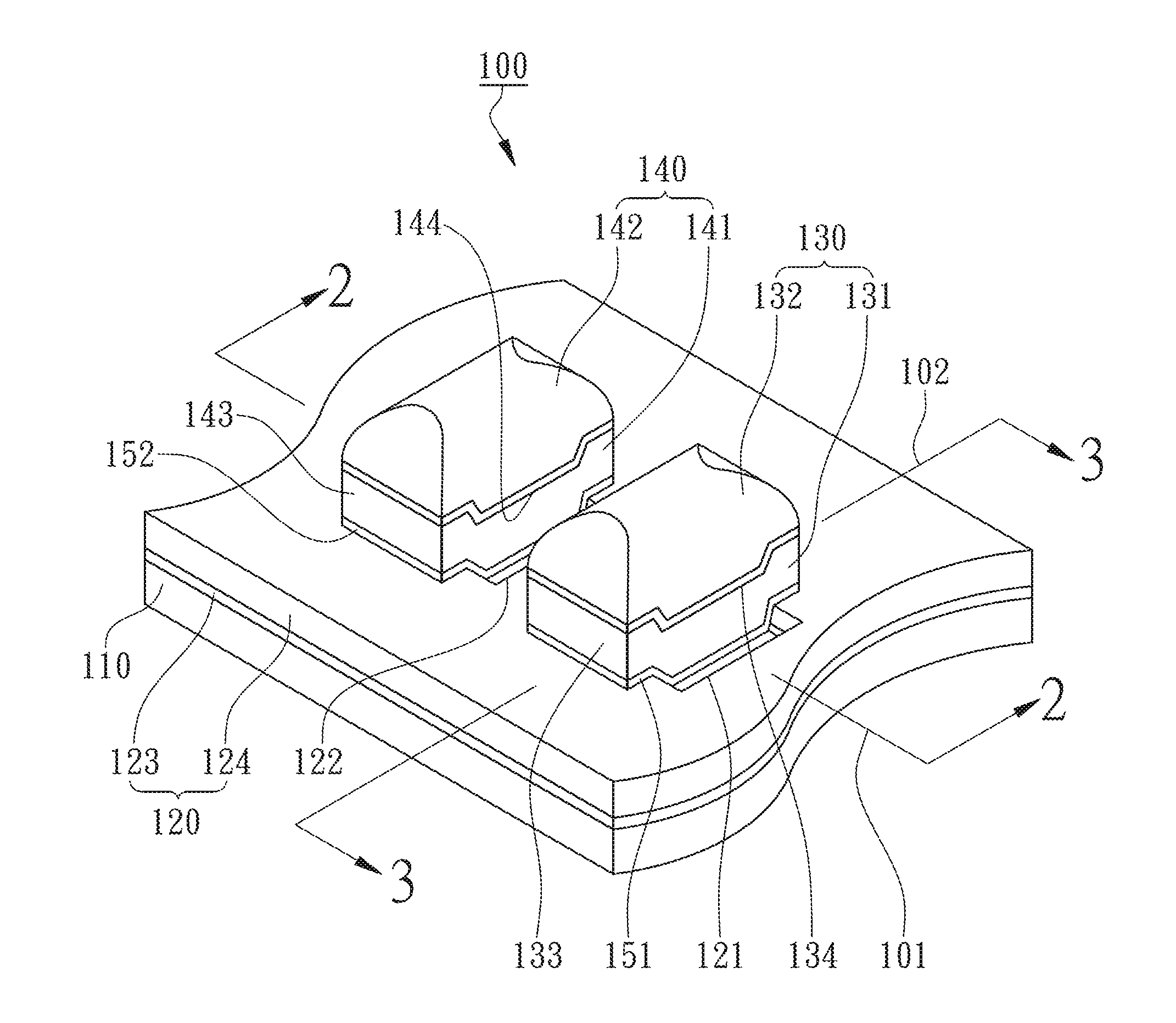
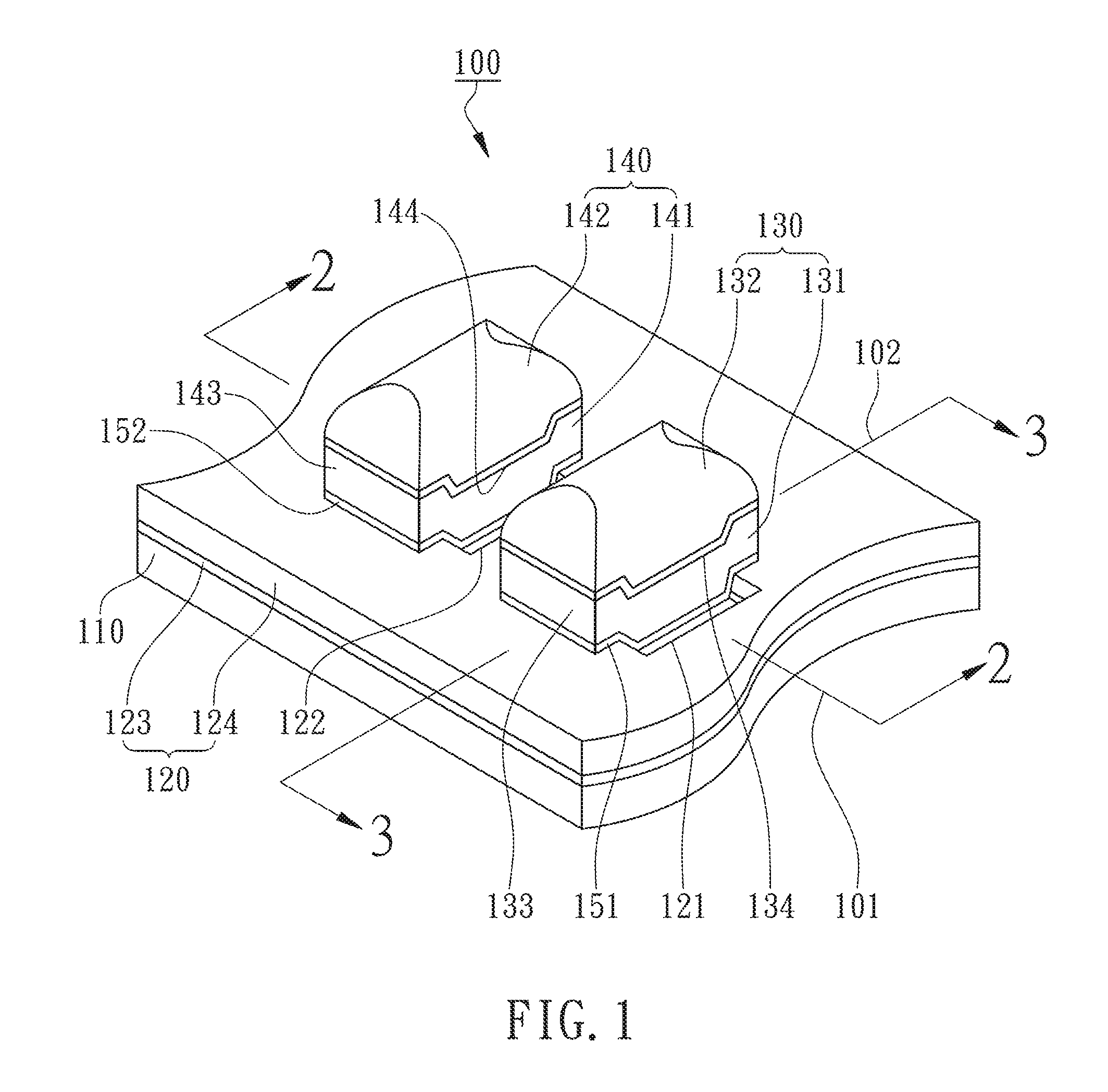
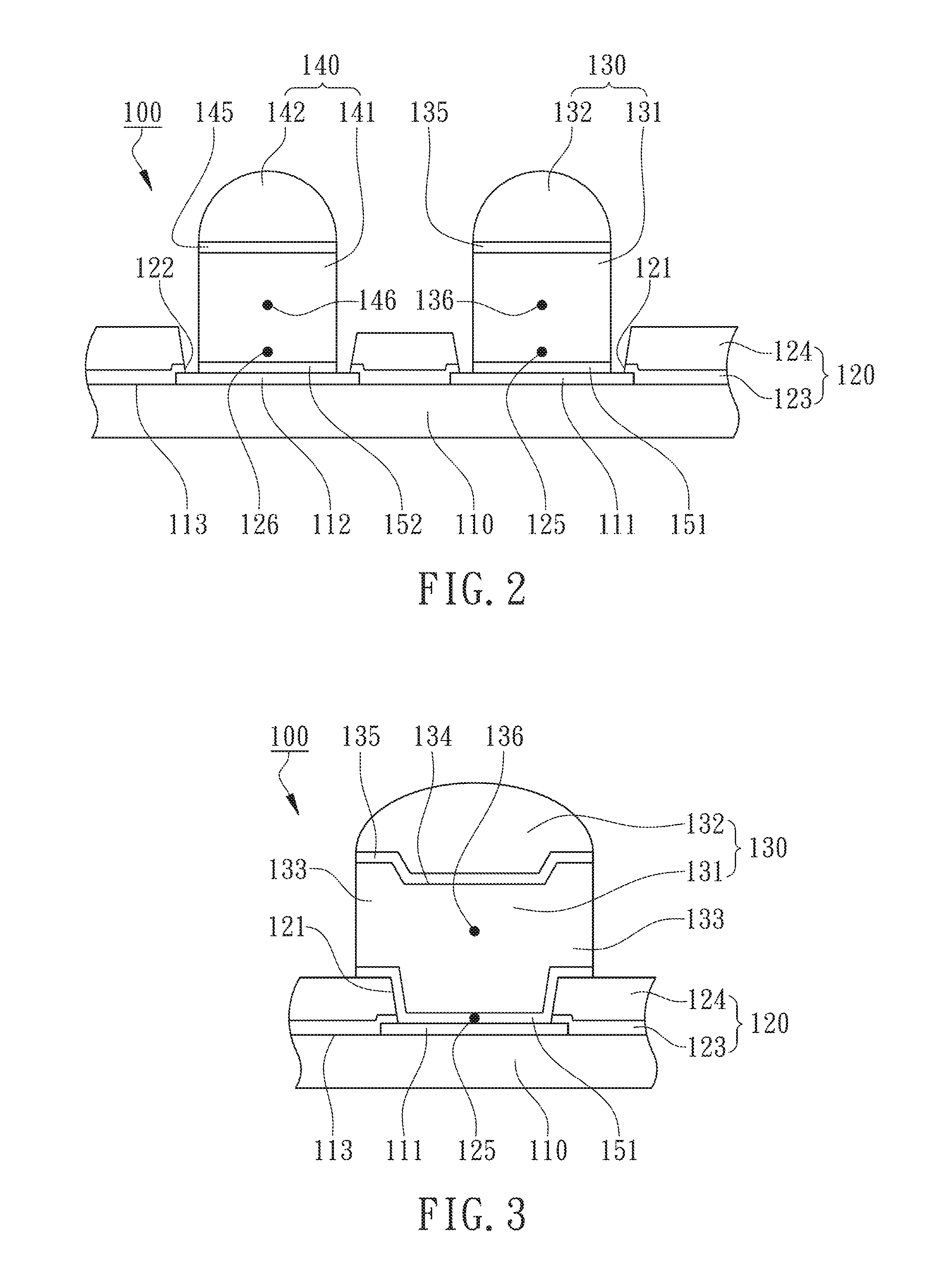
[0012]With reference to the attached drawings, the present invention is described by means of the embodiment(s) below where the attached drawings are simplified for illustration purposes only to illustrate the structures or methods of the present invention by describing the relationships between the components and assembly in the present invention. Therefore, the components shown in the figures are not expressed with the actual numbers, actual shapes, actual dimensions, nor with the actual ratio. Some of the dimensions or dimension ratios have been enlarged or simplified to provide a better illustration. The actual numbers, actual shapes, or actual dimension ratios can be selectively designed and disposed and the detail component layouts may be more complicated.

[0013]According to the preferred embodiment of the present invention, a fine-pitch pillar bump layout structure on chip is revealed and illustrated in FIG. 1 for a partial three-dimensional view, FIG. 2 for a cross-sectional ...


PUM


Abstract

Disclosed is a fine-pitch pillar bump layout structure on chip, comprising a chip, a passivation layer and at least two pillar bumps. Bonding pads of the chip are disposed along an X-axis. Openings of the passivation layer have a first aspect ratio. Pillar bumps are disposed on the bonding pads and each has a pillar body and a solder cap. Each pillar body has a plurality of symmetrical raised blocks disposed on the passivation layer and extended in both directions of Y-axis. The pillar bodies have shrunk bump widths along the X-axis so that a second aspect ratio is at least 1.5 times greater than the first aspect ratio and to partially expose the bonding pads and to make the central points of the pillar bodies be vertically aligned with the central points of the openings of the passivation layer.

Description

FIELD OF THE INVENTION[0001]The present invention relates to a layout structure of a bumped semiconductor device, more specifically to a fine-pitch pillar bump layout structure on chip.BACKGROUND OF THE INVENTION[0002]Most of the semiconductor devices such as DRAM has migrated from wire bonding interconnection to flip chip interconnection toward Wafer Level Chip Scale Packages (WLCSP). However, as the continuous die shrinkage with bonding pad miniaturization, fabrication of pillar bumps with solder caps such as Cu pillar bump (CPB) on fine-pitch bonding pad layout becomes more difficult where the bonding pad pitch is less than 80 μm. When flip-chip bonding a bumped chip, solder caps will easily bridge with the adjacent pillar bumps leading to electrical short. Moreover, encapsulation the gaps between bumped chips and substrates with underfill material after flip-chip bonding becomes more difficult. The conventional solution is to fabricate smaller pillar bumps, however, solder joint...

Claims


Application Information

Patent Timeline
Patent Type & Authority Applications(United States)
IPC IPC(8): H01L23/498
CPCH01L23/49811H01L2224/11H01L2224/1308H01L2224/13076H01L23/3192H01L24/13H01L24/14H01L2224/13013H01L2224/13021H01L2224/13022H01L2224/14517H01L2224/05567H01L2224/13111H01L2224/13147H01L2924/381H01L2924/3841H01L2924/00012H01L2924/00014H01L2924/01047H01L2924/01029
Inventor TAI, KUO-JUILIN, LI-JENHSU, SHOU-CHIAN
Owner POWERTECH TECHNOLOGY
Why Eureka
Try Eureka