

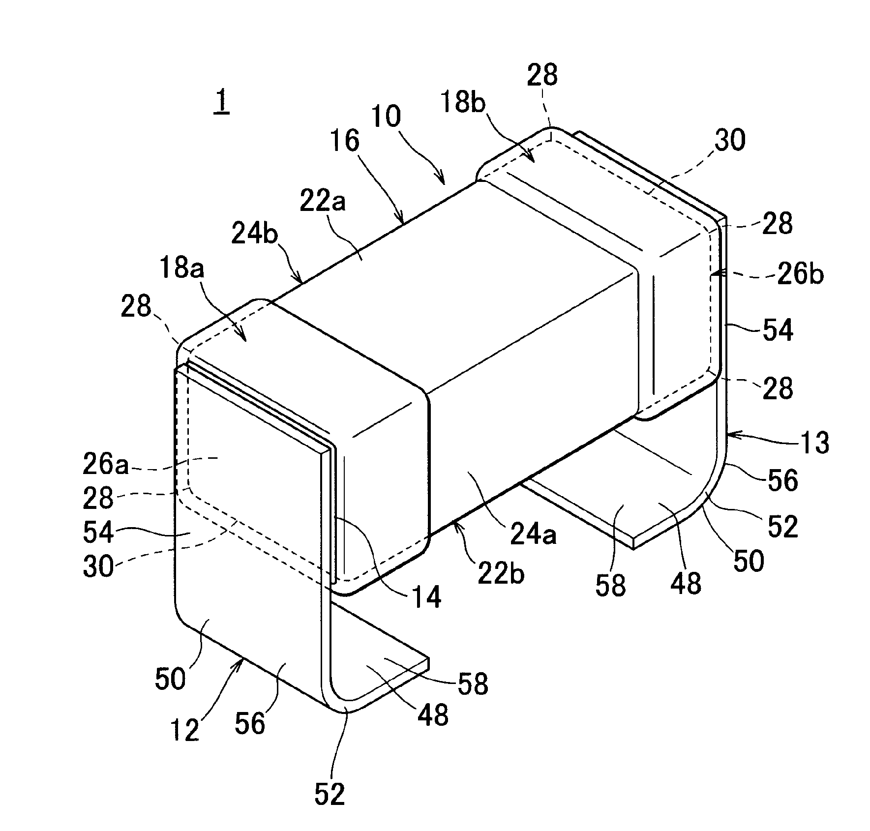
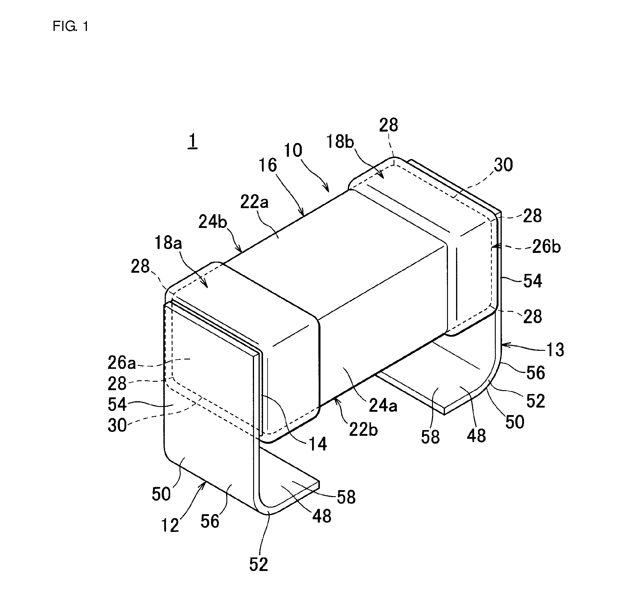
Ceramic electronic component
a technology of ceramic electronic components and components, applied in the direction of fixed capacitor details, generators/motors, fixed capacitors, etc., can solve the problems of mechanical distortion in ceramic layers, and achieve the effects of high melting point, low melting point, and high melting poin
- Summary
- Abstract
- Description
- Claims
- Application Information
AI Technical Summary
Benefits of technology
Problems solved by technology
Method used
Image

Examples
experimental examples
[0085]By using the ceramic electronic component obtained with the above-described method, an experiment was conducted to confirm whether the electronic component body was not detached from the metal terminals, displaced, or tilted in the reflow process when the ceramic electronic component was mounted to the mounting substrate. In the experiment conducted here, with intent to grasp an allowance in reflow heat resistance, a deviation in the bonded portion between the electronic component body and the metal terminal was examined by carrying out the reflow process in a loaded state (i.e., a state where another component serving as a weight is placed on the electronic component body). More specifically, a load chip (5750-size chip in this experiment) serving as a load was bonded to the upper surface of the ceramic electronic component according to the present preferred embodiment of the present invention by using a thermosetting adhesive. In such a state, the ceramic electronic componen...
PUM
| Property | Measurement | Unit |
|---|---|---|
| dielectric constant | aaaaa | aaaaa |
| dielectric constant | aaaaa | aaaaa |
| Thicknesses | aaaaa | aaaaa |
Abstract
Description
Claims
Application Information