Magnetic random access memory with switable switching assist layer

a random access memory and assist layer technology, applied in the field of sttmram elements, can solve the problems of devices that cannot scale beyond 65 nanometer (nm) process nodes, more complex cell architectures with high write current, and poor scalability attributed to the process used to manufacture these devices

Active Publication Date: 2015-03-05
AVALANCHE TECH
View PDF6 Cites 17 Cited by
  • Summary
  • Abstract
  • Description
  • Claims
  • Application Information

AI Technical Summary

Benefits of technology

[0023]FIG. 8 shows two graphs, 80 and 82, comparing the switching stability of a STTMRAM element of the embodiments of the present invention that do not include the materials and thicknesses indicated of the FL 28 vs. the switching stability of the STTMRAM element of the embodiments of the present invention that do include the materials and thicknesses indicated herein of the FL 28.

Problems solved by technology

The main hurdles associated with field-switched-MRAM are its more complex cell architecture with high write current (currently in the order of milliamps (mA)) and poor scalability attributed to the process used to manufacture these devices.
That is, these devices cannot scale beyond 65 nanometer (nm) process node.
The poor scalability of such devices is intrinsic to the field writing methods.
However, the problem with the element 10 as well as other prior art STTMRAM elements is that the level of electric current required to switch the magnetization orientation of FL 1 between parallel and anti-parallel relative to that of RL 3 is still higher than a typical semiconductor CMOS structure can provide, therefore making prior art STTMRAMs' applicability to storage systems not practical.

Method used


Image

  • Magnetic random access memory with switable switching assist layer
  • Magnetic random access memory with switable switching assist layer
  • Magnetic random access memory with switable switching assist layer

Examples


Embodiment Construction

[0034]In the following description of the embodiments, reference is made to the accompanying drawings that form a part hereof, and in which is shown by way of illustration of the specific embodiments in which the invention may be practiced. It is to be understood that other embodiments may be utilized because structural changes may be made without departing from the scope of the present invention. It should be noted that the figures discussed herein are not drawn to scale and thicknesses of lines are not indicative of actual sizes.

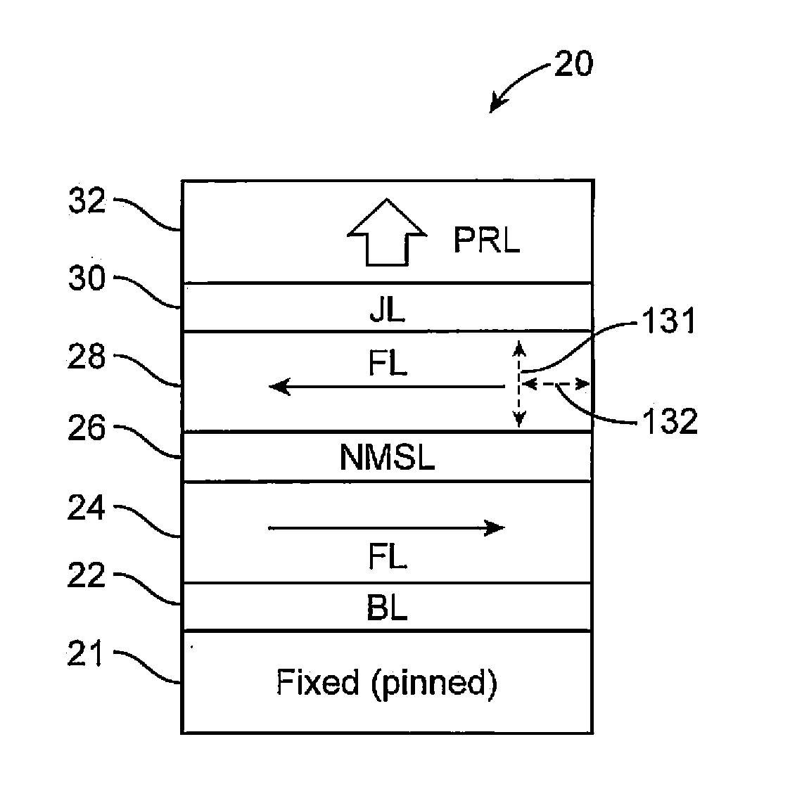
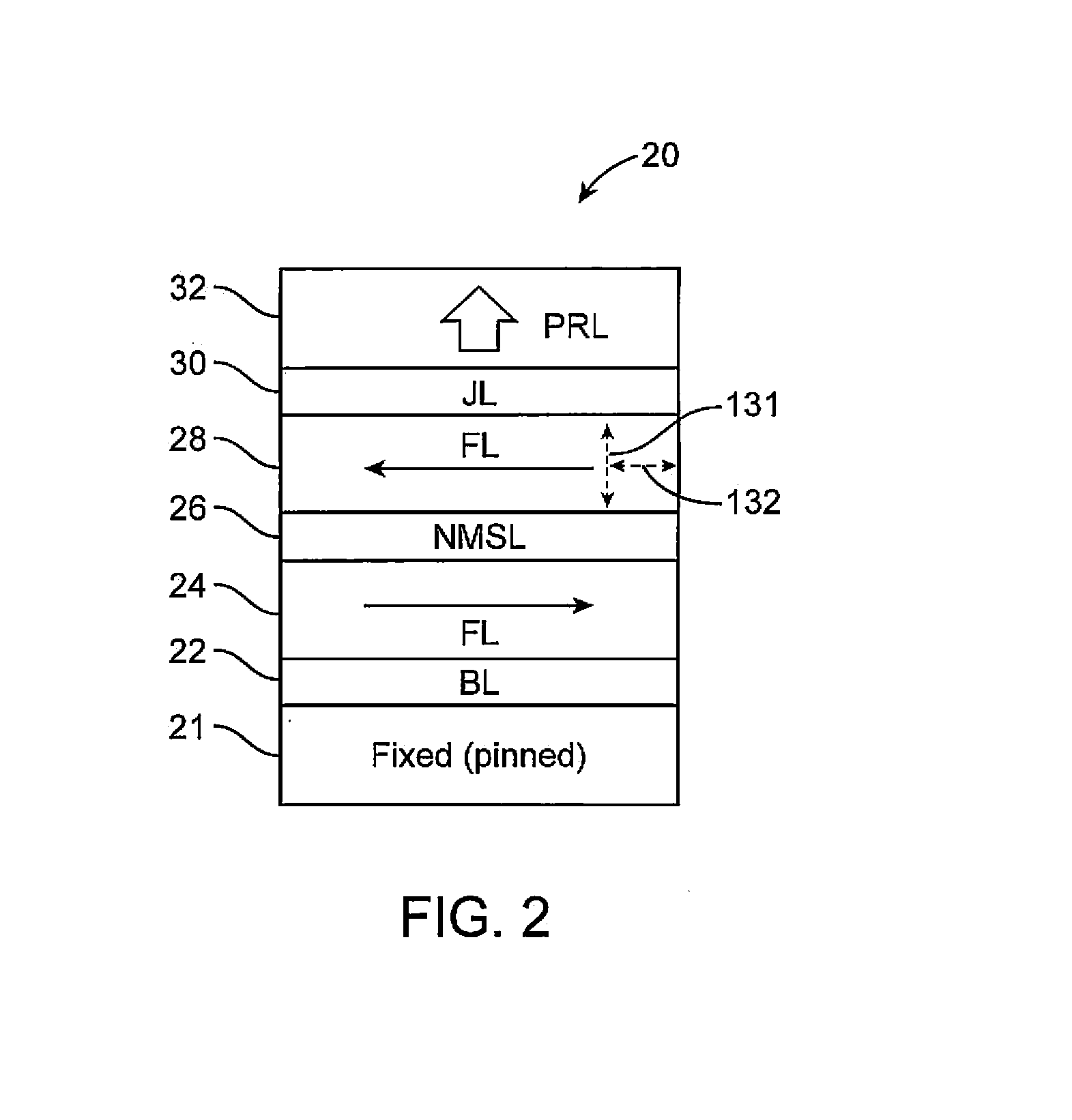
[0035]In the various STTMRAM elements to follow, a MTJ is employed with perpendicular magnetic anisotropy material(s) with improved stability in non-writing modes and easier switching during writing mode.

[0036]FIG. 2 shows relevant layers of a STTMRAM element 20 in accordance with an embodiment of the present invention. The STTMRAM element 20 is shown to include a fixed layer (sometimes referred to herein as a “reference layer (RL)”) 21 on top of which is ...


PUM


Abstract

A perpendicular spin-transfer torque magnetic random access memory (STTMRAM) element is configured to store a state when electrical current is applied thereto. The perpendicular STTMRAM element includes a magnetization layer having a first free layer and a second free layer, separated by a non-magnetic separation layer (NMSL). The direction of magnetization of the first and second free layers each is in-plane prior to the application of electrical current and after the application of electrical current, the direction of magnetization of the second free layer becomes substantially titled out-of-plane and the direction of magnetization of the first free layer switches. Upon electrical current being discontinued, the direction of magnetization of the second free layer remains in a direction that is substantially opposite to that of the first free layer.

Description

CROSS-REFERENCE TO RELATED APPLICATIONS[0001]This application is a continuation-in-part of previously-filed U.S. patent application Ser. No. 13 / 035,857, filed on Feb. 25, 2011, by Zhou et al., and entitled “Magnetic Latch Magnetic Random Access Memory (MRAM), which claims priority from previously-filed U.S. Provisional Application No. 61 / 391,263, filed on Oct. 8, 2010, by Huai et al. and entitled “Magnetic Latch Magnetic Random Access Memory (MRAM)”.BACKGROUND OF THE INVENTION[0002]1. Field of the Invention[0003]The present invention relates to a spin-transfer torque (STT) magnetic random access memory (MRAM), and, more particularly, to an STTMRAM element having magnetic tunnel junctions (MTJs) with a multi-layered free layer.[0004]2. Description of the Prior Art[0005]Magnetic random access memory (MRAM) is a type of non-volatile memory in which magnetization of magnetic layers in MTJs switches between parallel (corresponding to a low resistance state) and anti-parallel (correspondi...

Claims


Application Information

Patent Timeline
Patent Type & Authority Applications(United States)
IPC IPC(8): H01L43/10H01L43/02
CPCH01L43/02H01L43/10H01F10/123H01F10/3236H01F10/3254H01F10/3272H01F10/3286G11C11/161G11C11/1675G11C11/1659H10N50/85H10N50/10
Inventor ZHOU, YUCHENHUAI, YIMINGZHANG, JINGRANJAN, RAJIV YADAVMALMHALL, ROGER KLAS
Owner AVALANCHE TECH
Why Eureka
Try Eureka