Chip package structure and manufacturing method thereof

a technology of chip and packaging, applied in the direction of semiconductor devices, semiconductor/solid-state device details, electrical apparatus, etc., can solve the problems of non-conductive being unable to achieve the electro-magnetic interference shielding effect, wire breaking or damage, and inability to meet the requirements of miniaturization and mass production in low cost, etc., to achieve good electro-magnetic interference shielding, low manufacturing cost, and high assembly yield

Inactive Publication Date: 2015-03-19
CHIPMOS TECH INC
View PDF2 Cites 22 Cited by
  • Summary
  • Abstract
  • Description
  • Claims
  • Application Information

AI Technical Summary

Benefits of technology

[0006]The invention is directed to a chip package structure and a manufacturing method thereof, which have a high assembly yield, a low manufacturing cost and are good at electro-magnetic interference (EMI) shielding.

Problems solved by technology

Metal conductors are materials suitable for blocking the EMI, but the metal materials are heavy, uneasy to be shaped and in high price, hence they cannot satisfy the requirement of miniaturization and mass production in low cost.
However, the polymer material which is non-conductive is unable to achieve the electro-magnetic interference shielding effect.
In detail, the film layer is, for example, a film-over-wire (FOW), which presents a semi-solid gel state when the film layer encapsulates the chip and the wires, such that the wires may easily penetrate into the film layer without being interfered by the film layer, which may lead to wire breaking or damage.

Method used


Image

  • Chip package structure and manufacturing method thereof
  • Chip package structure and manufacturing method thereof
  • Chip package structure and manufacturing method thereof

Examples


Embodiment Construction

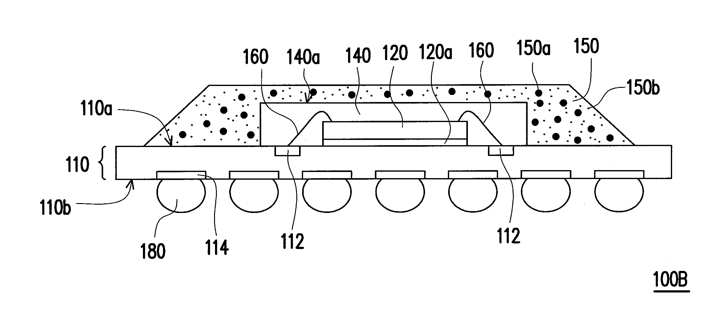
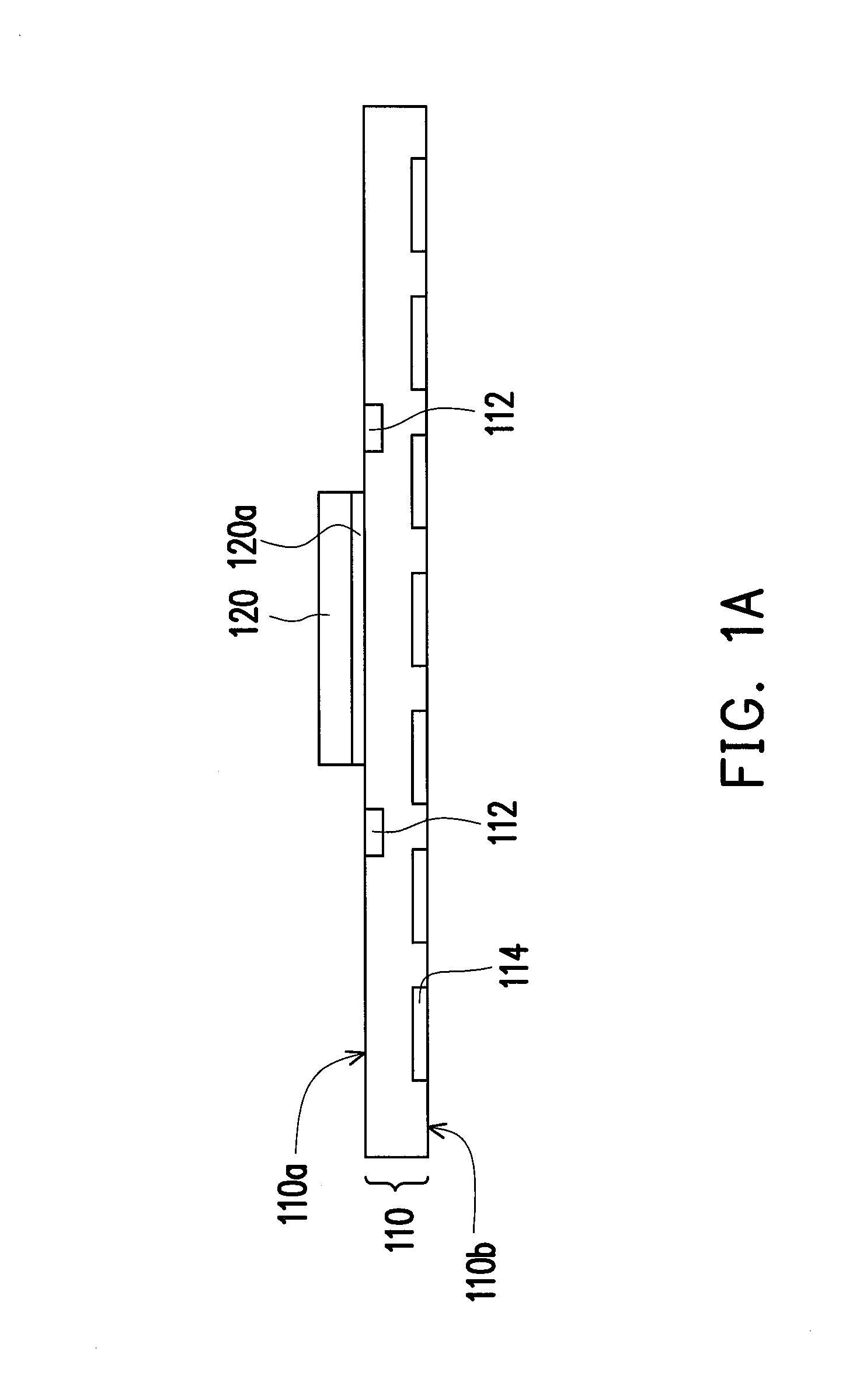
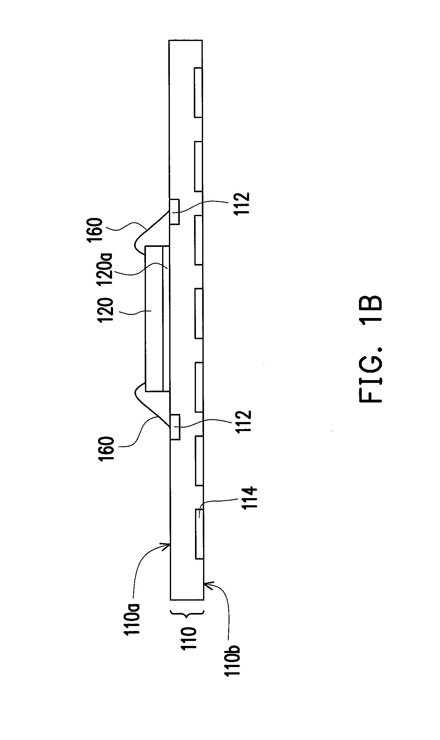
[0022]FIG. 1A-FIG. 1E are schematic diagrams of a packaging process of a chip package structure according to an embodiment of the invention. Referring to FIG. 1A, a substrate 110 is first provided, where the substrate 110 has an upper surface 110a and a lower surface 110b, and a chip 120 is mounted on the upper surface 110a of the substrate 110. In detail, the chip 120 is, for example, adhered to the upper surface 110a of the substrate 110 through an adhesive layer 120a. In the present embodiment, the substrate 110 is, for example, a multi-layer substrate fabricated according to a FR-4 substrate lamination technique or a ceramic substrate lamination technique, and the substrate 110 includes a plurality of pads 112 on the upper surface 110a of the substrate 110 and a plurality of pads 114 on the lower surface 110b of the substrate 110. On the other hand, the chip 120 can be an integrated circuit (IC) chip, for example, a graphics chip, a memory chip, a semiconductor chip or a driving...


PUM


Abstract

A chip package structure and a manufacturing method thereof are provided. The chip package structure includes a substrate, a chip, a plurality of wires, a film layer, a carrier, and an encapsulant. The substrate has an upper surface and a lower surface. The chip is mounted on the upper surface of the substrate. The wires are electrically connected to the chip and the substrate respectively. The film layer is attached to the substrate and entirely encapsulates the chip and the wires. The carrier is adhered on the film layer. The encapsulant is disposed on the upper surface of the substrate, wherein the encapsulant has an electro-magnetic shielding filler. The encapsulant at least partially encapsulates the carrier and the film layer, and the encapsulant covers the chip and the wires.

Description

CROSS-REFERENCE TO RELATED APPLICATION[0001]This application claims the priority benefit of Taiwan application serial no. 102133720, filed on Sep. 17, 2013. The entirety of the above-mentioned patent application is hereby incorporated by reference herein and made a part of this specification.BACKGROUND[0002]1. Technical Field[0003]The invention relates to a package structure and a manufacturing method thereof. Particularly, the invention relates to a chip package structure and a manufacturing method thereof.[0004]2. Related Art[0005]As electronic products are continually developed towards a trend of small size, multi-function and high performance, integrated circuit (IC) chips are also required to meet the requirements of miniaturization, high density, high power and high speed, so that a condition of electronic signals being influenced by electro-magnetic interference (EMI) is getting severer. In order to prevent the EMI from influencing the stability of the IC chip during operatio...

Claims


Application Information

Patent Timeline
Patent Type & Authority Applications(United States)
IPC IPC(8): H01L23/31H01L23/373H01L21/56H01L23/00H01L23/552H01L23/433
CPCH01L23/3157H01L2224/485H01L23/4334H01L21/56H01L24/83H01L24/48H01L23/3736H01L2924/01079H01L2924/01029H01L2924/01047H01L2924/01013H01L2924/01046H01L2224/8385H01L2224/48227H01L2224/48091H01L23/552H01L23/3121H01L23/3135H01L23/3737H01L23/49816H01L24/29H01L24/32H01L24/45H01L24/73H01L24/92H01L2224/2919H01L2224/32225H01L2224/45124H01L2224/45139H01L2224/45144H01L2224/45147H01L2224/45164H01L2224/73265H01L2224/83192H01L2224/92247H01L2924/14H01L2924/1434H01L2924/15311H01L2924/181
Inventor PAN, YU-TANGCHOU, SHIH-WEN
Owner CHIPMOS TECH INC
Why Eureka
Try Eureka