
Apparatus and Method for a Boost Converter with Improved Electrical Overstress (EOS) Tolerance

a technology of electrical overstress and amplifier, applied in the direction of power conversion systems, electric variable regulation, instruments, etc., can solve the problems of single component electrical overstress events, and failures that can be detected and controlled, and achieve good resilience to failures

Inactive Publication Date: 2015-03-19
DIALOG SEMICONDUCTOR GMBH
View PDF4 Cites 16 Cited by
  • Summary
  • Abstract
  • Description
  • Claims
  • Application Information

AI Technical Summary

Benefits of technology

The patent aims to provide a circuit device that has strong resistance to electrical overstress and is highly efficient in power utilization.

Problems solved by technology

Given that the voltage or current conditions exceed the component's electrical safe operating area (E-SOA) or thermal safe operating area (T-SOA), latent or destructive failure can occur.
In power converters, voltage conditions that can exceed the native technology voltage leading to over-voltage and over-stress conditions.
Charged cables can lead to electrical overstress events in single components, or integrated circuits mounted on printed circuit boards.
If the switch is cycled quickly, the inductor does not have enough time to fully discharge.
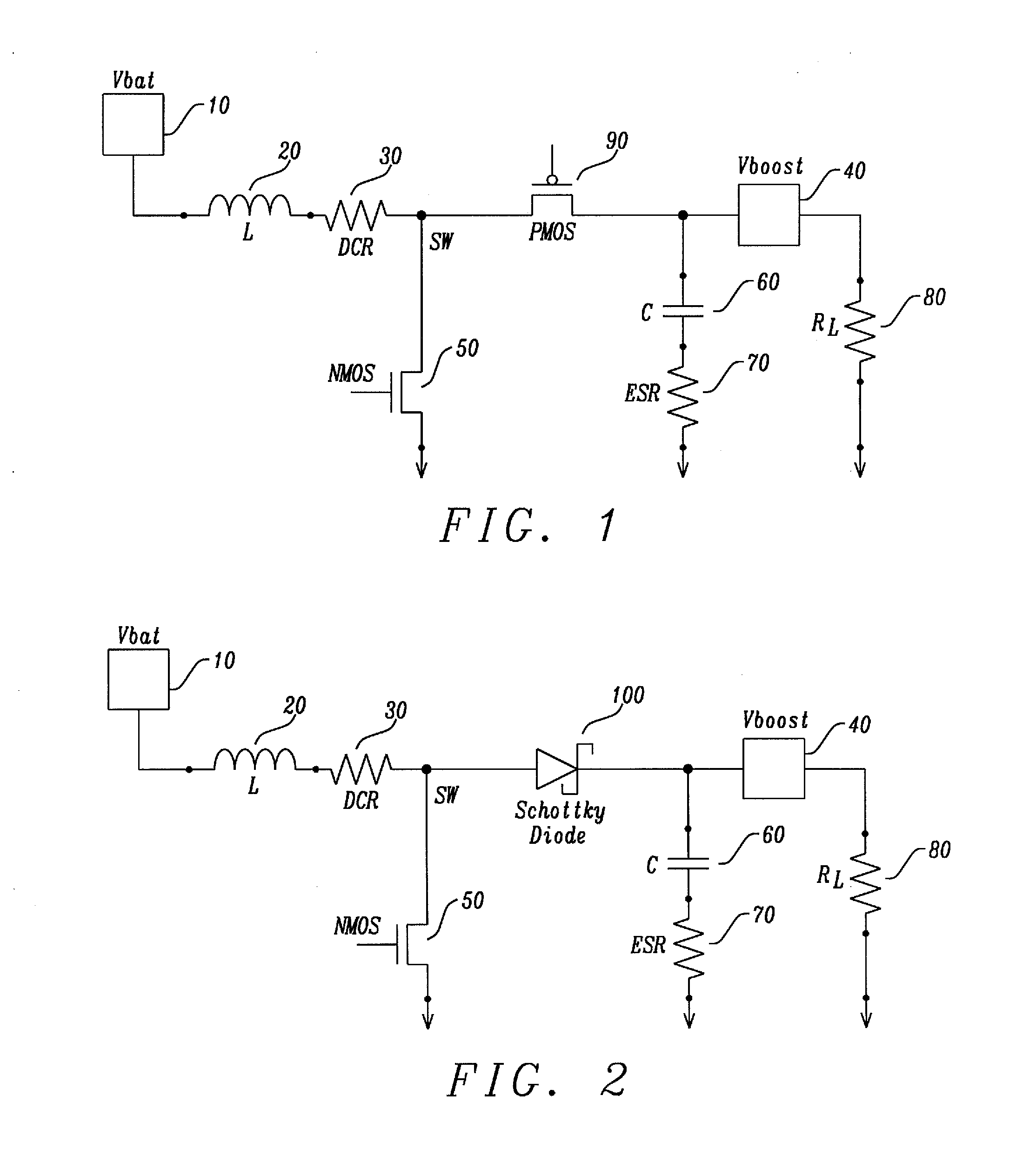
In the prior art, as illustrated in FIG. 1, and FIG. 2, the boosted power converter has the disadvantage that it cannot discharge the output voltage Vboost if it rises significantly.
Both the passive and active elements in the circuit are vulnerable to electrical overstress (EOS).
A solution to avoid electrical overstress (EOS) in this application is achieved by adding off-chip external clamping diodes to limit the boost voltage; this is a disadvantage due to the added area as well as extra component cost to the printed circuit board (PCB).
As shown, the prior art implementation of a DC-to-DC boost power converter can lead to electrical over-stress (EOS) of the passive and active elements.
This solution adds significant complexity and area to the boost power converter.
The addition of “off-chip” external components to address electrical overstress (EOS) is a disadvantage due to the additional cost of the external components, weight of the external components, and the area on the printed circuit boards (PCB).
For automotive, aerospace, and military applications, the area and weight of the off-chip elements can be a disadvantage.
For handheld devices, portables, and laptop applications, the additional components impact size, area, and cost of the application.

Method used


Image

  • Apparatus and Method for a Boost Converter with Improved Electrical Overstress (EOS) Tolerance
  • Apparatus and Method for a Boost Converter with Improved Electrical Overstress (EOS) Tolerance
  • Apparatus and Method for a Boost Converter with Improved Electrical Overstress (EOS) Tolerance

Examples


Embodiment Construction

[0038]FIG. 1 is a circuit schematic diagram illustrating a prior art embodiment of a boost converter with a p-channel MOS (PMOS) field effect switch. A first switch to the ground node to activate the current flow into the inductor L 20, where the switch is an n-channel metal oxide semiconductor (NMOS) field effect transistor device 50. The capacitor element can be represented by an ideal capacitor element 60 and its electrical series resistance (ESR) 70. A load element can be illustrated as a resistor element, RL 80. A second “switch” is illustrated in FIG. 1 in series with the inductor and the load elements, where the switch is a p-channel metal oxide semiconductor (PMOS) field effect transistor device 90. In this illustrated implementation, by utilizing a PMOS field effect transistor device, the “switching” of the transistor can be controlled at the PMOS gate electrode. In this prior art embodiment, the passive capacitor element 60 and active PMOS switch 90 can undergo electrical ...


PUM


Abstract

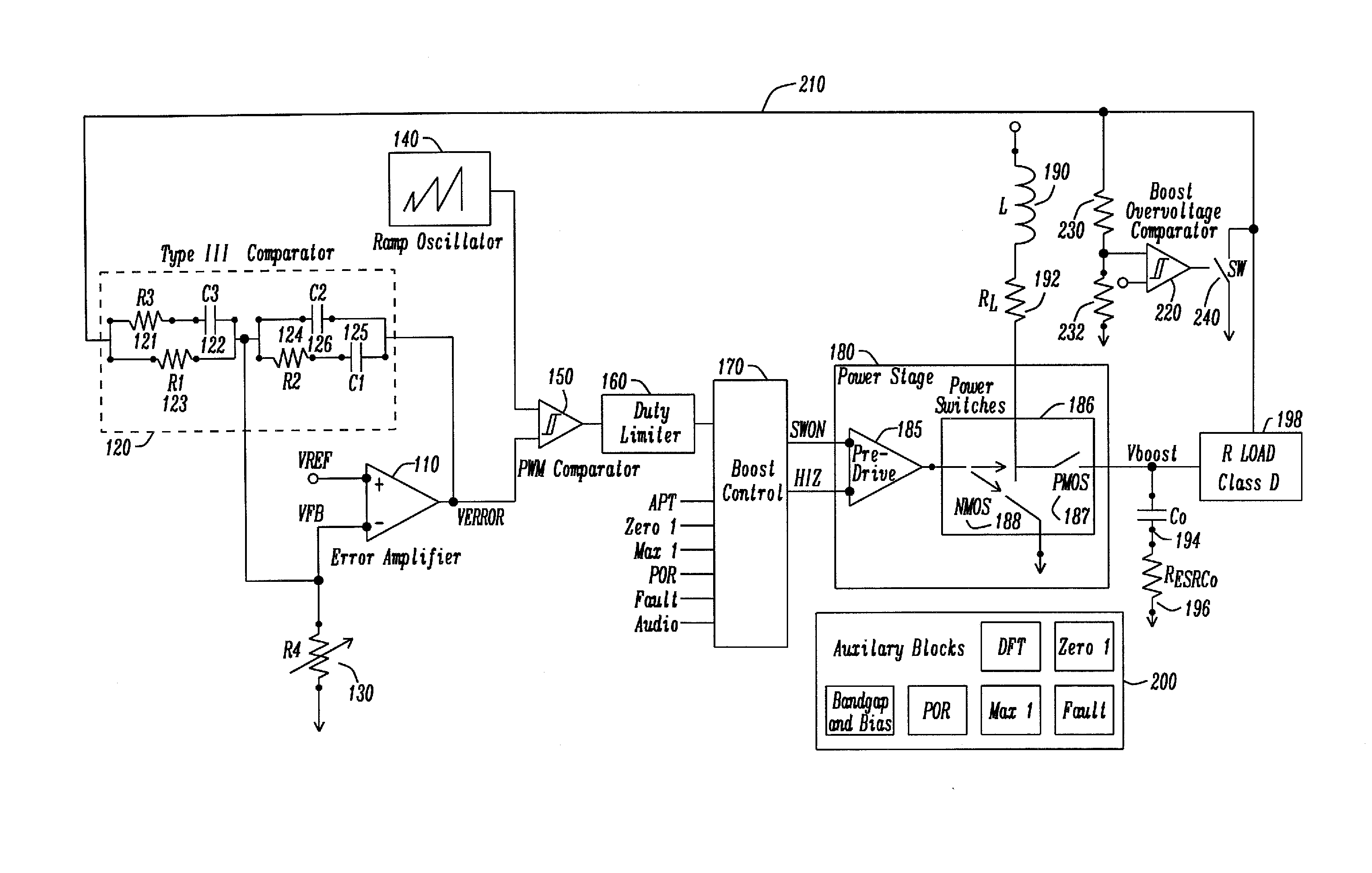
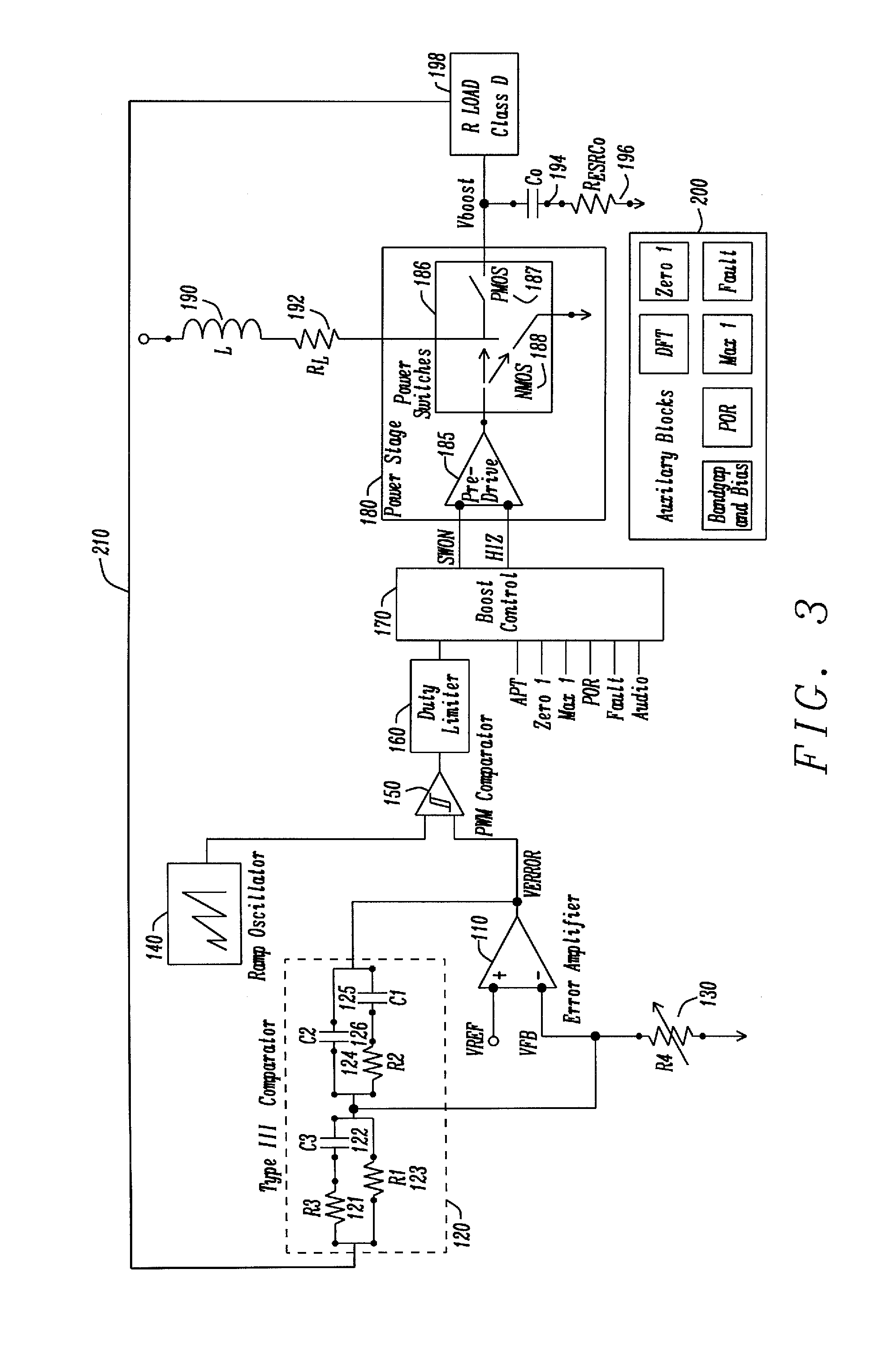
An apparatus and method for a boost power converter with improved electrical overstress (EOS) tolerance is disclosed. A boost power converter provides a providing a pulse width modulation (PWM) boost power converter with an electrical overstress (EOS) boost over-voltage comparator / switch network comprises a boost power converter, a boost overvoltage comparator, a boost overvoltage comparator feedback network, and a boost overvoltage switch. The methodology for the boost converter with improved electrical overstress (EOS) tolerance defines an absolute maximum voltage condition, provides a voltage limit below the defined absolute maximum voltage condition, and initiates turn-on of the boost overvoltage switch according to the voltage limit.

Description

BACKGROUND[0001]1. Field[0002]The disclosure relates generally to a power converter circuits, and more particularly, to a DC-to-DC boost power converter circuit device having improved electrical overstress (EOS) tolerance thereof.[0003]2. Description of the Related Art[0004]DC-to-DC power converters are used to provide voltage conditions that are different than the voltage of a given input source. DC-to-DC power converters can provide an output voltage greater, equal, or lower than the input voltage. A boost converter (also known as a step-up converter) is a DC-to-DC power converter whose output voltage is greater than its input voltage. A buck converter (also known as a step-down converter) is a DC-to-DC power converter whose output voltage is lower than its input voltage. A buck-boost converter is a DC-to-DC power converter whose output voltage magnitude is either greater than or less than the input voltage magnitude. Boost, buck, and buck-boost converters are different classes of...

Claims


Application Information

Patent Timeline
IPC IPC(8): H02M3/156H02M1/32
CPCH02M1/32H02M3/156H02M3/158H02M1/0041
Inventor KILIC, YAVUZ
Owner DIALOG SEMICONDUCTOR GMBH
Learn More