

Electromagnetic interference shielding material, electromagnetic interference shielding device, method for making the electromagnetic interference shielding device, electromagnetic interference shielding package module and appliance
a technology electromagnetic interference, applied in the field of electromagnetic interference shielding materials, can solve the problems of increasing thickness, further downsizing of appliances, and portions unshielded, and achieve the effects of maintaining effective electromagnetic interference shielding, reducing viscosity, and effectively limiting the thickness of package modules
- Summary
- Abstract
- Description
- Claims
- Application Information
AI Technical Summary
Benefits of technology
Problems solved by technology
Method used
Image

Examples
embodiment 1
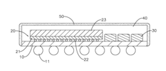
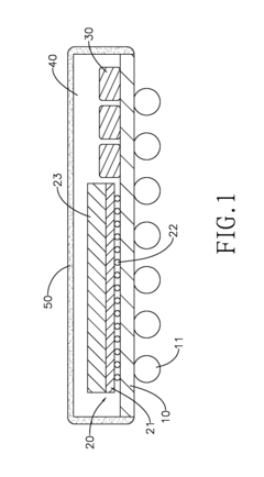
[0022]With reference to FIG. 1, an embodiment in accordance with the present invention to be hereinafter described relates to an EMI shielding device, which was made from the EMI shielding material in accordance with the present invention, implemented to an EMI shielding package module of an appliance.
[0023]The EMI shielding package module comprises a package body and a thin film shaped EMI shielding device 50.
[0024]The package body comprises a packaging material 40 and at least one electronic unit. The at least one electronic unit is to be packaged within the packaging material 40 with the connectivity to the outer environment of the electronic unit being maintained. The electronic unit is a unit susceptible to EMI that requires proper shielding, such as a radio frequency identification (RFID) unit, a wireless communication unit, or a signal-receiving unit. In the instant embodiment, a chip 20 and multiple inner units 30 constitute an electronic unit to be packaged in the packaging...
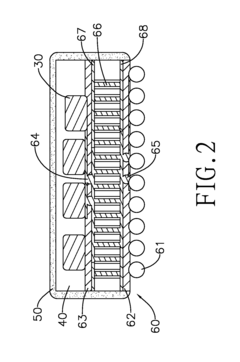
embodiment 2
[0034]With reference to FIG. 2, the instant embodiment demonstrates another mode of practice in accordance with the present invention, The instant embodiment is largely the same as the foregoing embodiment 1, except that the instant embodiment employs a through-silicon via (TSV) chip 60, instead of a chip 20 as described in Embodiment 1. The chip 20 used in Embodiment 1, which comprises the chip-substrate 21 and chip-solder balls 22, demands a considerable space. In contrast, the TSV chip 60, which is capable of building multi-dimensional connections via guide holes 66, helps to save space taken by the chip-substrate 21 and the chip-solder balls 22. The structure of the TSV chip 60 thus forms a three-dimensional structure which is densely structured and significantly contributes to down-sizing of appliances. The instant embodiment comprises the aforementioned TSV chip 60. The TSV chip 60 comprises multiple guide holes 66. The guide holes 66 communicate between a chip bottom 62 and a...
embodiment 3
[0036]With reference to FIG. 3, the instant embodiment demonstrates the application of the present invention to an antenna module 70, suitable examples of which include a ZigBee wireless communication module. The antenna module 70 comprises an antenna circuit 71 and a controlling circuit 72. The controlling circuit 72 comprises at least one electronic unit. In the instant embodiment, the controlling circuit 72 comprises a first electronic unit 73 and a second electronic unit 74. The first electronic unit 73 and the second electronic unit 74 are packaged with the aforementioned EMI shielding material and the foregoing TSV chip is employed, so as to contribute to down-sizing.
[0037]Specifically, the antenna module 70 is packaged by means of large scale integration (LSE) or surface-mount technology (SMT) to form a package body with a protective insulating resin. The package body is then spread with the aforementioned EMI shielding material for shielding from EMI and thus completes a pac...
PUM
| Property | Measurement | Unit |
|---|---|---|
| Temperature | aaaaa | aaaaa |
| Temperature | aaaaa | aaaaa |
| Length | aaaaa | aaaaa |
Abstract
Description
Claims
Application Information