Semiconductor laser device assembly

a semiconductor laser and laser technology, applied in the direction of laser optical resonator construction, laser details, nanotechnology, etc., can solve the problems of high energy efficiency, difficult for large-scale resonators to realize mechanical stability, and high cost of titanium/sapphire lasers, etc., to achieve high peak output, increase the average output of laser beam output from semiconductor laser elements to the outside, and reduce the cost of a system

Active Publication Date: 2015-03-26
SONY CORP
View PDF4 Cites 12 Cited by
  • Summary
  • Abstract
  • Description
  • Claims
  • Application Information

AI Technical Summary

Benefits of technology

[0017]In the semiconductor laser device assembly according to the first aspect of the present disclosure, the extension direction of the diffraction surface of the diffraction grating and the main vibration direction of the field of the laser beam incident on the diffraction grating are substantially parallel to each other. In addition, in the semiconductor laser device assembly according to the second aspect of the present disclosure, the extraction efficiency of the laser beam component having the field of which the vibration direction is included in the plane parallel to the principal surface of the semiconductor laser element to the outside is higher than the extraction efficiency of the laser beam component having the field of which the vibration direction is included in the plane orthogonal to the principal surface of the semiconductor laser element to the outside. For this reason, an average output of the laser beam output from the semiconductor laser element to the outside can be increased. In addition, because a pulse laser having a high peak output in a 400 nm wavelength band can be realized by a mode synchronization semiconductor laser element, the spread of an ultrashort pulse light source of femtosecond order can be promoted, a pulse laser of several tens of watts or more can be realized by a mode synchronization semiconductor laser element simple substance, and downsizing and cost reduction of a system can be realized.

Problems solved by technology

However, the titanium / sapphire laser is expensive and is a large-scale solid-state laser light source, which results in becoming a main factor that disturbs a technical spread.
In addition, a different solid-state laser to oscillate consecutive light is necessary for excitation and energy efficiency is not necessarily high.
Besides, it is not easy for a large-scaled resonator to realize mechanical stability and specialized knowledge is required on maintenance.

Method used


Image

  • Semiconductor laser device assembly
  • Semiconductor laser device assembly
  • Semiconductor laser device assembly

Examples


second example (modification of the first example)

3. Second example (modification of the first example)

third example (another modification of first example)

4. Third example (another modification of first example)

5. Fourth example (modifications of the first to third examples) and others

[Overall Description of Semiconductor Laser Device Assemblies According to First and Second Aspects of Present Disclosure]

[0035]As a method of generating a light pulse having a time width of about several picoseconds using a semiconductor laser element, a mode synchronization method is known. In the mode synchronization method, active mode synchronization in which gain or loss is modulated at a cycle equal to a lap time in an external resonator structure and passive mode synchronization in which a saturable absorber showing a non-linear optical response is provided in the semiconductor laser element and is operated exist. However, the passive mode synchronization is more suitable for generating a light pulse having a pulse time width of about several picoseconds or less. In a semiconductor laser device assembly according to a first aspect or a second asp...

first example

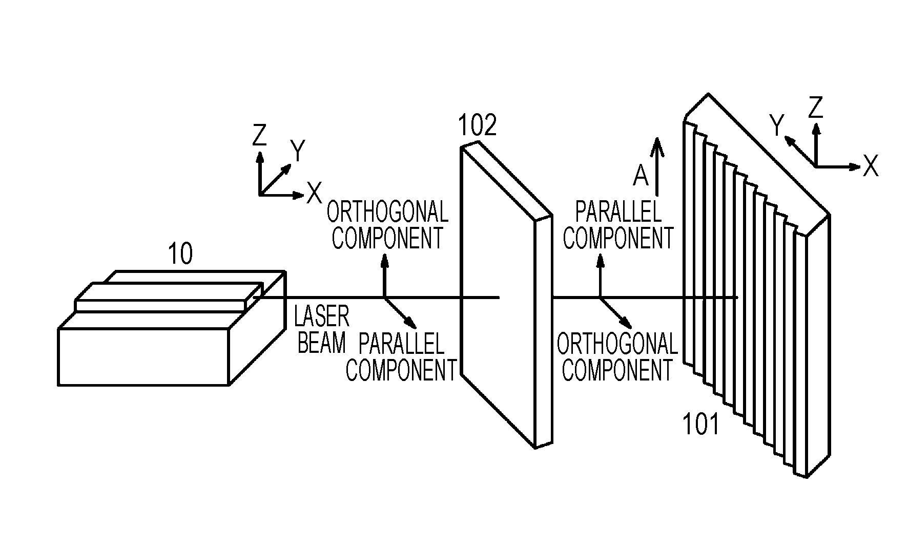
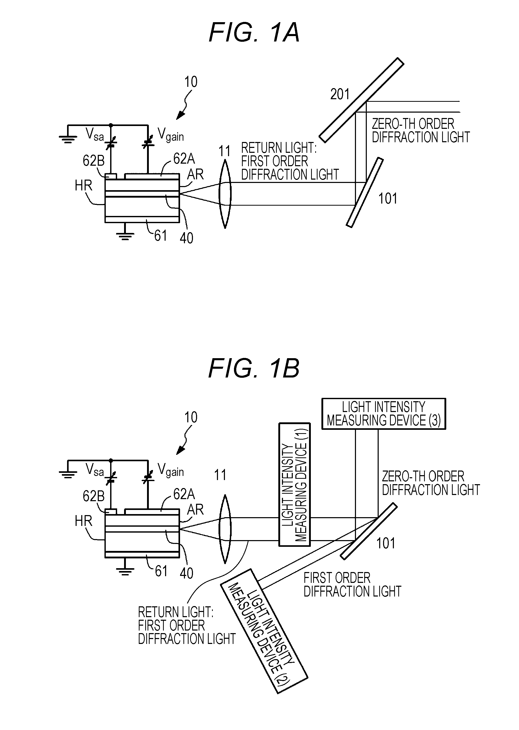
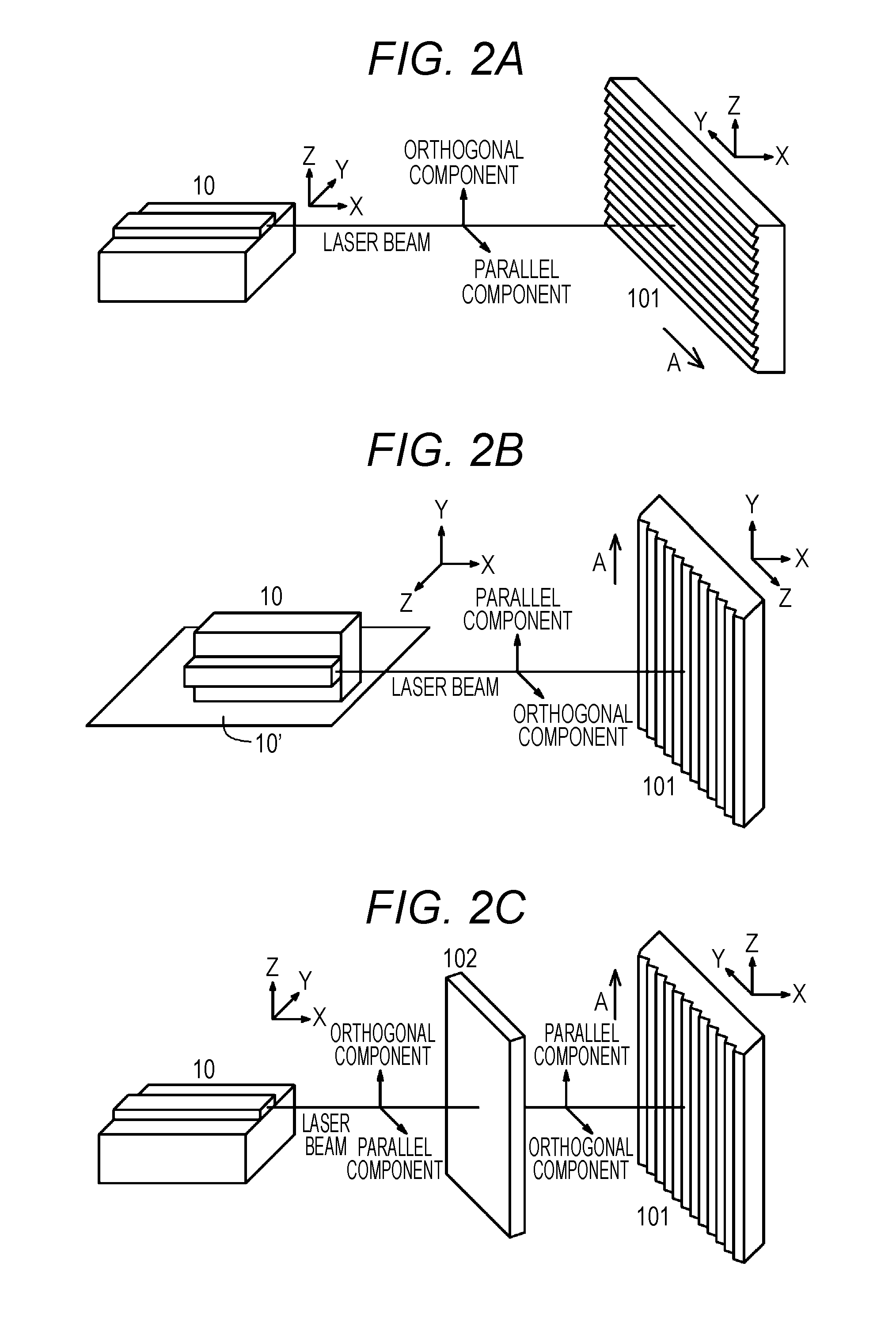
[0092]A first example relates to a semiconductor laser device assembly according to the first aspect and the second aspect of the present disclosure. A conceptual diagram of the semiconductor laser device assembly according to the first example is illustrated in FIG. 1A, an arrangement state of a semiconductor laser element and a diffraction grating or an optical element is schematically illustrated in FIG. 2A, 2B, or 2C, a schematic cross-sectional view along an extension direction of a resonator of the semiconductor laser element is illustrated in FIG. 6, and a schematic cross-sectional view along a direction perpendicular to the extension direction of the resonator of the semiconductor laser element is illustrated in FIG. 7.

[0093]The semiconductor laser device assembly according to the first example or second to fourth examples to be described below includes (A) a semiconductor laser element and (B) a diffraction grating 101 that configures an external resonator, returns diffract...


PUM


Abstract

A semiconductor laser device assembly includes (A) a semiconductor laser element and (B) a diffraction grating that configures an external resonator, returns diffraction light other than zero-th order diffraction light to the semiconductor laser element, and outputs the zero-th order diffraction light to the outside. An extension direction of a diffraction surface of the diffraction grating and a main vibration direction of a field of a laser beam incident on the diffraction grating are substantially parallel to each other.

Description

TECHNICAL FIELD[0001]The present disclosure relates to a semiconductor laser device assembly.BACKGROUND ART[0002]Recently, an ultrashort pulse / ultrahigh output laser has been actively used for making a study of an advanced scientific domain using a laser beam where a pulse time width is at an atto-second level or a femtosecond level. In addition, in the ultrashort pulse laser, in addition to a scientific interest called the elucidation of ultrafast phenomena such as picoseconds and femtoseconds, an application study to practical use such as minute processing or two-photon imaging has been actively performed using high peak power. In addition, a high-output ultrashort-pulse semiconductor laser element that is configured from a GaN compound semiconductor and has a light emission wavelength in a 405 nm band has been expected as a light source of a volume-type optical disk system expected as a next-generation optical disk system following a Blu-ray optical disk system, a light source re...

Claims


Application Information

Patent Timeline
Patent Type & Authority Applications(United States)
IPC IPC(8): H01S5/12
CPCH01S5/12H01S3/105H01S5/0657H01S5/101H01S5/141H01S5/143H01S5/22H01S5/3216H01S5/34333B82Y20/00H01S5/06253H01S5/323H01S5/14H01S5/32341
Inventor WATANABE, HIDEKIKONO, SHUNSUKEKURAMOTO, MASARU
Owner SONY CORP
Why Eureka
Try Eureka