Thin film semiconductor device and manufacturing method therefor
a thin film semiconductor and manufacturing method technology, applied in the direction of semiconductor devices, electrical appliances, transistors, etc., can solve the problems of oxide semiconductor damage and degraded characteristics, and achieve the effect of stable characteristics and thin film
- Summary
- Abstract
- Description
- Claims
- Application Information
AI Technical Summary
Benefits of technology
Problems solved by technology
Method used
Image

Examples
first embodiment
Organic EL Display Device
[0079]First, a structure of an organic EL display device 10 according to a first embodiment is described with reference to FIG. 4. FIG. 4 is a perspective partially cutaway view of an organic EL display device according to this embodiment.
[0080]As shown in FIG. 4, the organic EL display device 10 has a multilayered structure that includes a TFT substrate (TFT array substrate) 20 in which plural thin film transistors are arranged and organic EL elements (emitting portions) 40. The organic EL elements each have an anode 41 which is a lower electrode, an EL layer 42 which is an emitting layer composed of an organic material, and a cathode 43 which is a transparent upper electrode.
[0081]In the TFT substrate 20, plural pixels 30 are arranged in a matrix and one pixel circuit 31 is provided for each of the pixels 30.
[0082]The organic EL elements 40 are formed to respectively correspond to the pixels 30. The pixel circuit 31 of each of the pixels 30 controls emissi...
second embodiment
[0180]Next, a second embodiment is described. An organic EL display device according to this embodiment has the same structure as the organic EL display device 10 of the first embodiment. Thus, the description therefor is omitted to avoid redundancy. A thin film semiconductor device is described below.
Thin Film Semiconductor Device
[0181]A thin film semiconductor device according to this embodiment will now be described. A thin film semiconductor device according to this embodiment is a bottom-gate, channel-etch thin film transistor.
[0182]FIG. 14 is a schematic cross-sectional view of a thin film semiconductor device according to this embodiment.
[0183]As shown in FIG. 14, a thin film semiconductor device 200 according to this embodiment includes a substrate 110, a gate electrode 120, a gate insulating film 130, an oxide semiconductor layer 240, a channel protective layer 250, a source electrode 260s, and a drain electrode 260d. The oxide semiconductor layer 240 includes an oxygen ric...
third embodiment
[0201]Next, a third embodiment is described. An organic EL display device according to this embodiment has the same structure as the organic EL display device 10 of the first embodiment. Thus, the description therefor is omitted to avoid redundancy. A thin film semiconductor device is described below.
Thin Film Semiconductor Device
[0202]A thin film semiconductor device of this embodiment will now be described. A thin film semiconductor device according to this embodiment is a top-gate thin film transistor.
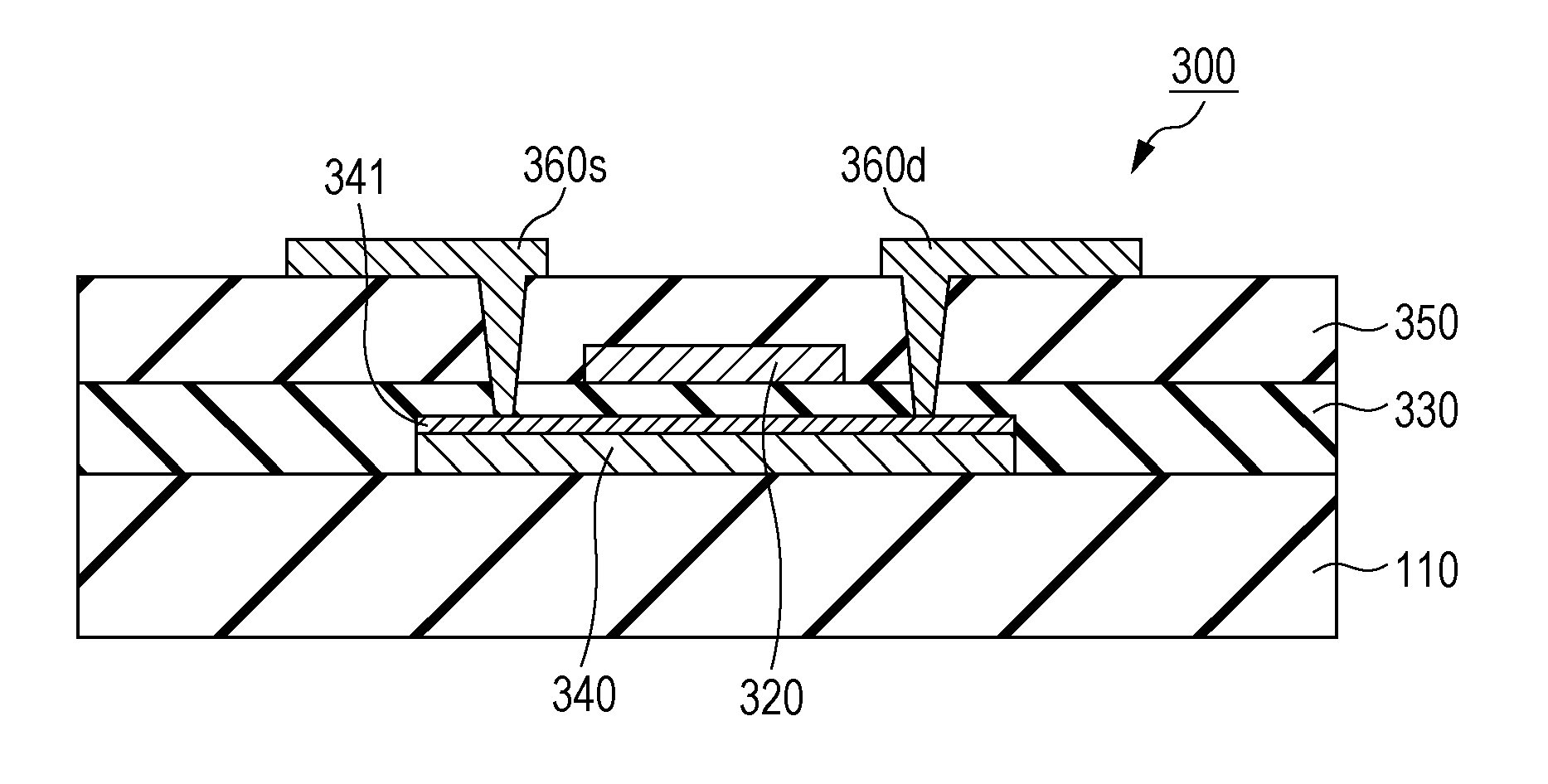
[0203]FIG. 16 is a schematic cross-sectional view of a thin film semiconductor device according to this embodiment.
[0204]As shown in FIG. 16, a thin film semiconductor device 300 according to this embodiment includes a substrate 110, a gate electrode 320, a gate insulating film 330, an oxide semiconductor layer 340, an insulating layer 350, a source electrode 360s, and a drain electrode 360d. The oxide semiconductor layer 340 includes an oxygen rich layer 341. Some structures that a...
PUM
 Abstract
Description
Claims
Application Information
 - R&D
- Intellectual Property
- Life Sciences
- Materials
- Tech Scout
- Unparalleled Data Quality
- Higher Quality Content
- 60% Fewer Hallucinations
Browse by: Latest US Patents, China's latest patents, Technical Efficacy Thesaurus, Application Domain, Technology Topic, Popular Technical Reports.
© 2025 PatSnap. All rights reserved.Legal|Privacy policy|Modern Slavery Act Transparency Statement|Sitemap|About US| Contact US: help@patsnap.com