
Electronic component unit and manufacturing method therefor

Active Publication Date: 2015-04-09
MURATA MFG CO LTD
View PDF9 Cites 6 Cited by
  • Summary
  • Abstract
  • Description
  • Claims
  • Application Information

AI Technical Summary

Benefits of technology

The patent text discusses how to reduce the size of electronic components by reducing the distance between the component and the side surface of the substrate. This is achieved by allowing for a certain amount of extra space between the component and the first side surface, which can be different from the distance between the second side surface and the component. By doing this, the size of the electronic component unit is reduced.

Problems solved by technology

Thus, even if the size of a component to be mounted is reduced, there is a limitation on reducing the size of an electronic component unit including such a component mounted on a substrate.

Method used


Image

  • Electronic component unit and manufacturing method therefor
  • Electronic component unit and manufacturing method therefor
  • Electronic component unit and manufacturing method therefor

Examples


first preferred embodiment

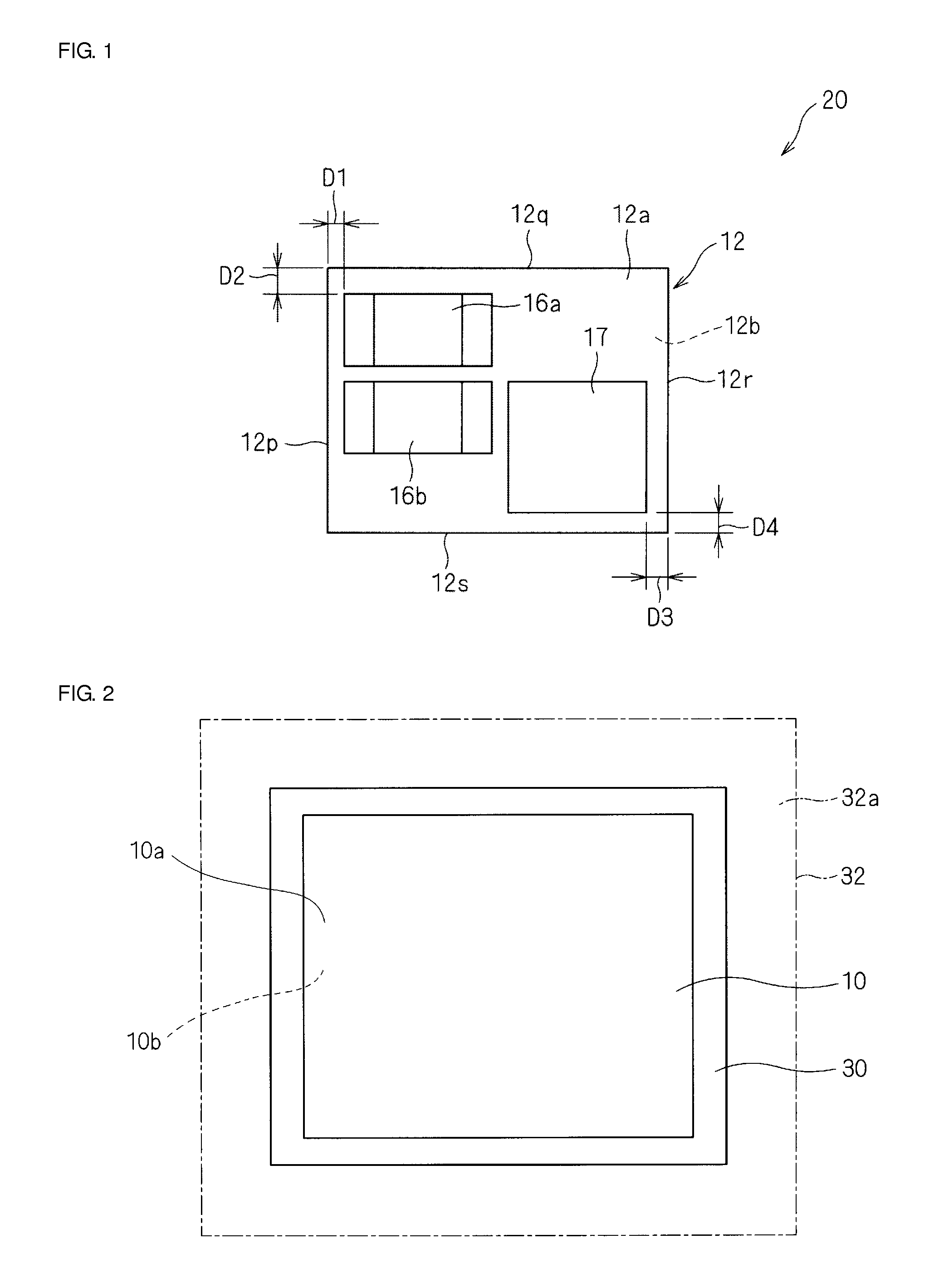
[0047]An electronic component unit 20 according to a first preferred embodiment of the present invention will be described below with reference to FIGS. 1 through 4.

[0048]FIG. 1 is a plan view of the electronic component unit 20. As shown in FIG. 1, in the electronic component unit 20, components 16a, 16b, and 17 are mounted on a substrate 12.

[0049]The substrate 12 includes a pair of rectangular or substantially rectangular principal surfaces 12a and 12b opposing each other and side surfaces 12p through 12s connecting between the principal surfaces 12a and 12b. As the substrate 12, a printed board using phenolic paper or glass epoxy resin, a flexible board using polyimide, liquid crystal polymer, or polyester, or a ceramic board may preferably be used.

[0050]The components 16a, 16b, and 17 to be mounted are chip components 16a and 16b, such as a chip capacitor, for example, a multilayer ceramic capacitor, a chip resistor, a chip coil, a chip vibrator, a chip protection element, and a...

second preferred embodiment

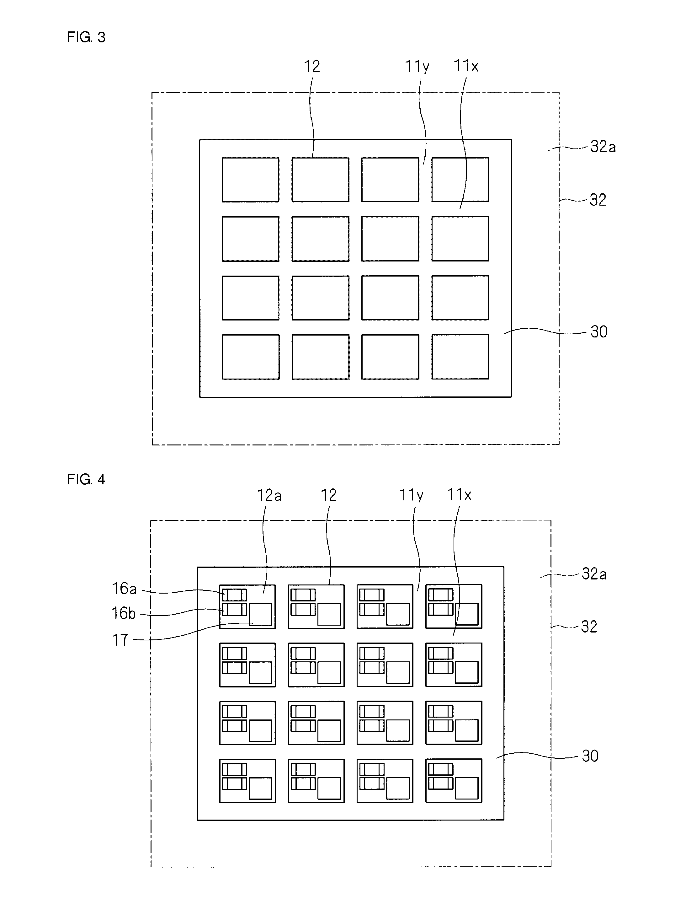
[0061]A non-limiting example of a manufacturing method for the electronic component unit 20 according to a second preferred embodiment of the present invention will be discussed below with reference to FIGS. 1 and 5 through 8.

[0062]In the second preferred embodiment, the electronic component unit 20 having the same configuration as the first preferred embodiment shown in FIG. 1 is fabricated by using a manufacturing method different from that of the first preferred embodiment, as shown in FIGS. 5 through 8. FIGS. 5 through 8 are plan views schematically illustrating manufacturing steps for the electronic component unit 20.

[0063]First, as shown in FIG. 5, an aggregate substrate 10s is prepared and is temporarily fixed. The aggregate substrate 10s includes a pair of principal surfaces 10a and 10b opposing each other. One principal surface 10b of the aggregate substrate 10s is temporarily fixed to a plane 32a of a jig 32 by using adhesive tape 30. The aggregate substrate 10s may be tem...

third preferred embodiment

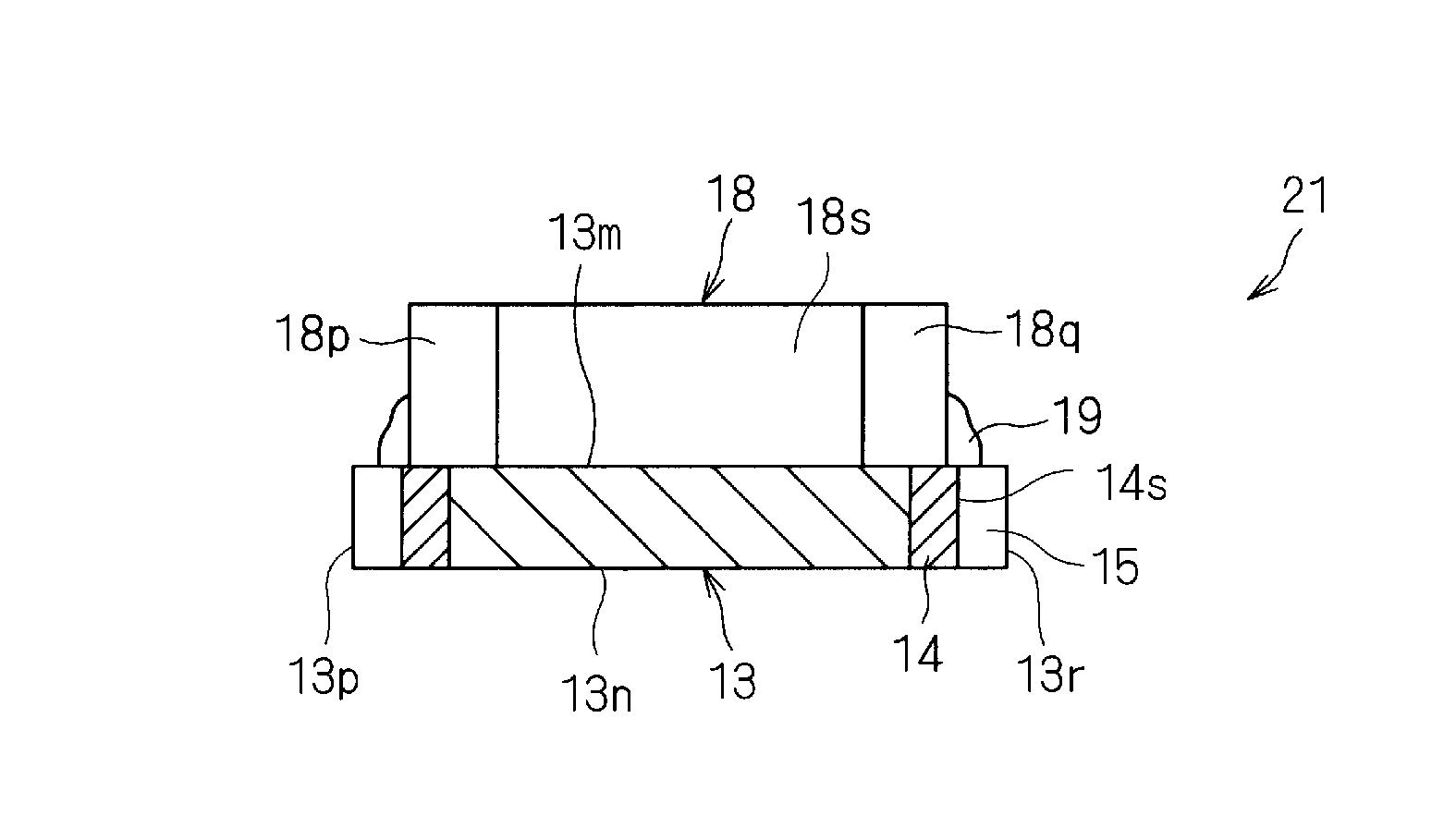
[0075]An electronic component unit 21 according to a third preferred embodiment of the present invention will be described below with reference to FIGS. 9, 10A and 10B.

[0076]FIG. 10A is a plan view of the electronic component unit 21. FIG. 10B is a sectional view taken along line X-X of FIG. 10A.

[0077]As shown in FIGS. 10A and 10B, the electronic component unit 21 preferably is an interposer capacitor including a multilayer capacitor 18 mounted on an interposer substrate 13. The multilayer capacitor 18 is configured such that electrodes 18p and 18q are provided at both ends of a rectangular body 18s, and is mounted by using a bonding medium 19, such as solder or a conductive paste. The interposer substrate 13 includes a pair of rectangular or substantially rectangular principal surfaces 13m and 13n opposing each other and side surfaces 13p through 13s connecting between the principal surfaces 13m and 13n. The side surfaces 13q and 13s along the long sides of the principal surfaces 1...


PUM

PropertyMeasurementUnit
Distanceaaaaaaaaaa

Abstract

An electronic component unit includes a substrate including principal surfaces opposing each other and side surfaces between the principal surfaces, and components mounted on the principal surface of the substrate. The side surfaces include first side surfaces formed before the components are mounted and second side surfaces formed after the components are mounted. As viewed from a line normal to the principal surface of the substrate, distances between the first side surfaces and the components are different from distances between the second side surfaces and the components.

Description

BACKGROUND OF THE INVENTION[0001]1. Field of the Invention[0002]The present invention relates to an electronic component unit and a manufacturing method therefor, and more particularly, to an electronic component unit including a component mounted on a substrate and to a manufacturing method for such an electronic component unit.[0003]2. Description of the Related Art[0004]Hitherto, various electronic component units including components mounted on substrates have been proposed.[0005]For example, in an interposer capacitor 101 shown in a plan view of FIG. 12, a multilayer capacitor 102 is mounted on an interposer substrate 120. The interposer substrate 120 has the function of reducing vibration which may be conducted to, for example, a circuit board on which the interposer capacitor 101 is mounted, by absorbing vibration generated in the multilayer capacitor 102 due to the application of an AC voltage.[0006]By using an aggregate substrate including individual substrate regions to be...

Claims


Application Information

Patent Timeline
IPC IPC(8): H01G2/06H05K1/18H01G4/12H05K3/30H01G4/30
CPCH01G2/065H05K3/303H05K2201/10015H01G4/12H05K1/181H01G4/30H01G2/06H05K1/111H05K3/0052H05K3/0097H05K2201/09063H05K2201/09227H05K2201/2045Y02P70/50Y10T29/4913
Inventor OGAWA, KAZUTOKATO, ISAO
Owner MURATA MFG CO LTD
Features
  • Generate Ideas
  • Intellectual Property
  • Life Sciences
  • Materials
  • Tech Scout
  • Unparalleled Data Quality
  • Higher Quality Content
  • 60% Fewer Hallucinations
Learn More