Electrically insulating thermal interface on the discontinuity of an encapsulation structure

a technology of discontinuity and encapsulation structure, which is applied in the direction of semiconductor devices, semiconductor/solid-state device details, electrical apparatus, etc., can solve the problems affecting the dielectric strength of electronic semiconductor packages, and achieve good thermally conductive materials, effective thermal balance, and large effective surface area

Active Publication Date: 2015-04-16
INFINEON TECH AG
View PDF38 Cites 23 Cited by
  • Summary
  • Abstract
  • Description
  • Claims
  • Application Information

AI Technical Summary

Benefits of technology

[0010]One exemplary embodiment has the advantage that, by covering (in particular, filling) a discontinuity at the encapsulation structure with material of the thermal interface structure, the path length (“creeping distance”), over which an electrical leakage current has to travel in order to reach the carrier with the electronic chip mounted thereon from the exterior of the electronic semiconductor package actually covered by the thermal interface structure, is increased significantly. In other words, the length of the current path, which a leakage current has to overcome in order to propagate between the surroundings of the electronic semiconductor package and the interior of the electronic semiconductor package, is increased. This leads to an increase in the dielectric strength and to an improvement in the electronic performance of the electronic semiconductor package. The formation of the discontinuity and covering the same with the thermal interface material effects an improved adhesion of the thermal interface structure to the encapsulation structure due to the increased contact surface, whereby the susceptibility of the electronic semiconductor package to leakage current is further reduced. The measures described also render the electronic semiconductor package and, in particular, its package, suitable for use with particularly high electric voltages, which is extremely advantageous, particularly in the area of semiconductor components with power chips. According to the exemplary embodiment described, a robust semiconductor package can be made available, which provides a reliable electrical insulation, even under stress or with a high mechanical or electrical load. The reliable and secure attachment of the thermal interface structure to the encapsulation structure thus increases the operational reliability of the electronic semiconductor package.DESCRIPTION OF FURTHER EMBODIMENTS
[0044]According to an exemplary embodiment, the encapsulation structure can have multiple discontinuities, which are at least partially filled by the electrically insulating thermal interface structure. By providing multiple discontinuities, the properties in respect of the leakage current behavior and the adhesion can be further improved.

Problems solved by technology

With an undesirable delaminating of the thermal interface material from the encapsulation structure, disruptive leakage currents can form between the surroundings of the electronic semiconductor package and the electrical carrier coupled to an electronic chip, which affect the dielectric strength of the electronic semiconductor package.

Method used


Image

  • Electrically insulating thermal interface on the discontinuity of an encapsulation structure
  • Electrically insulating thermal interface on the discontinuity of an encapsulation structure
  • Electrically insulating thermal interface on the discontinuity of an encapsulation structure

Examples


Embodiment Construction

[0011]Additional exemplary embodiments of the electronic semiconductor package, the electronic arrangement and the method for manufacturing an electronic semiconductor package are described in the following.

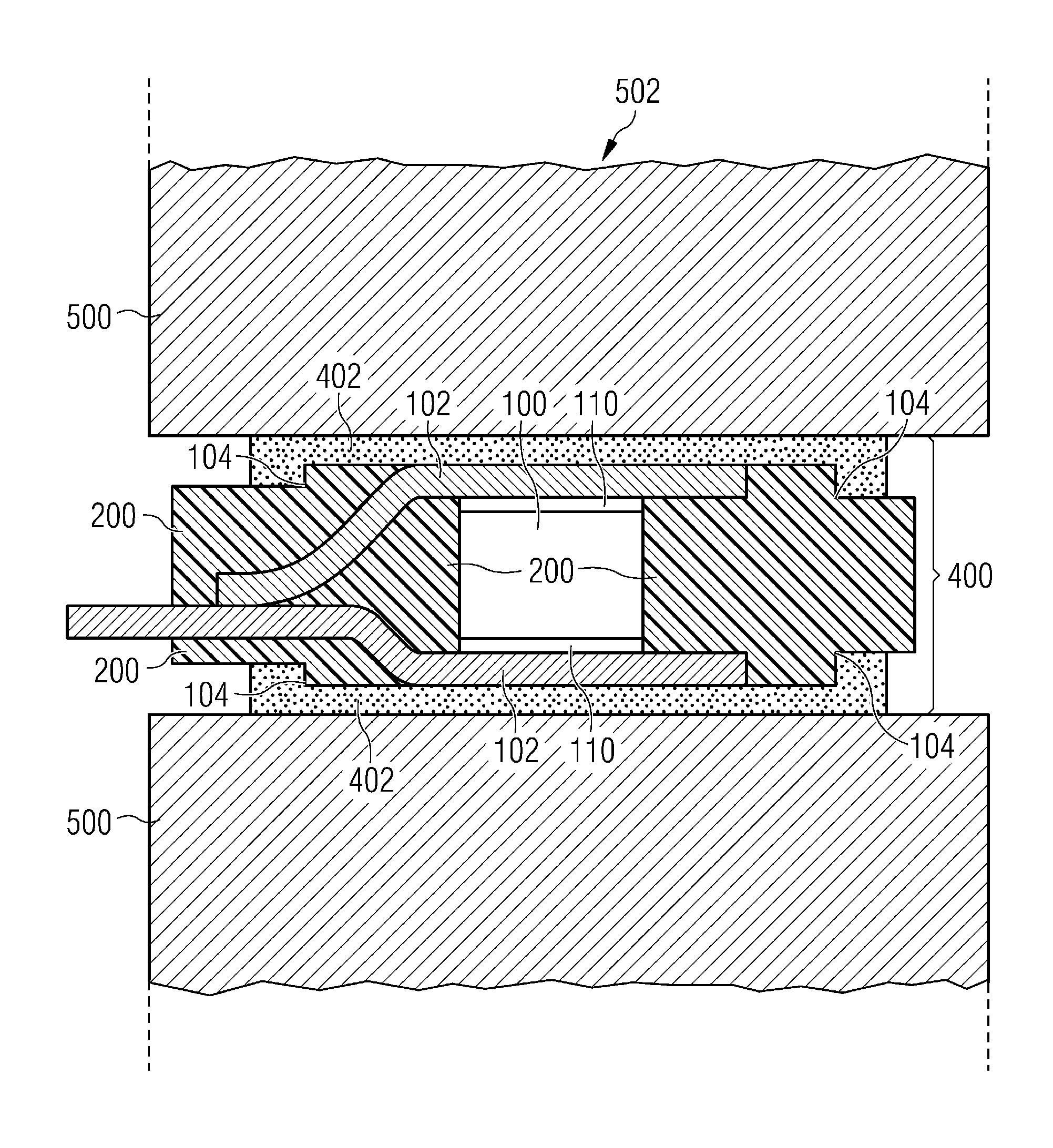
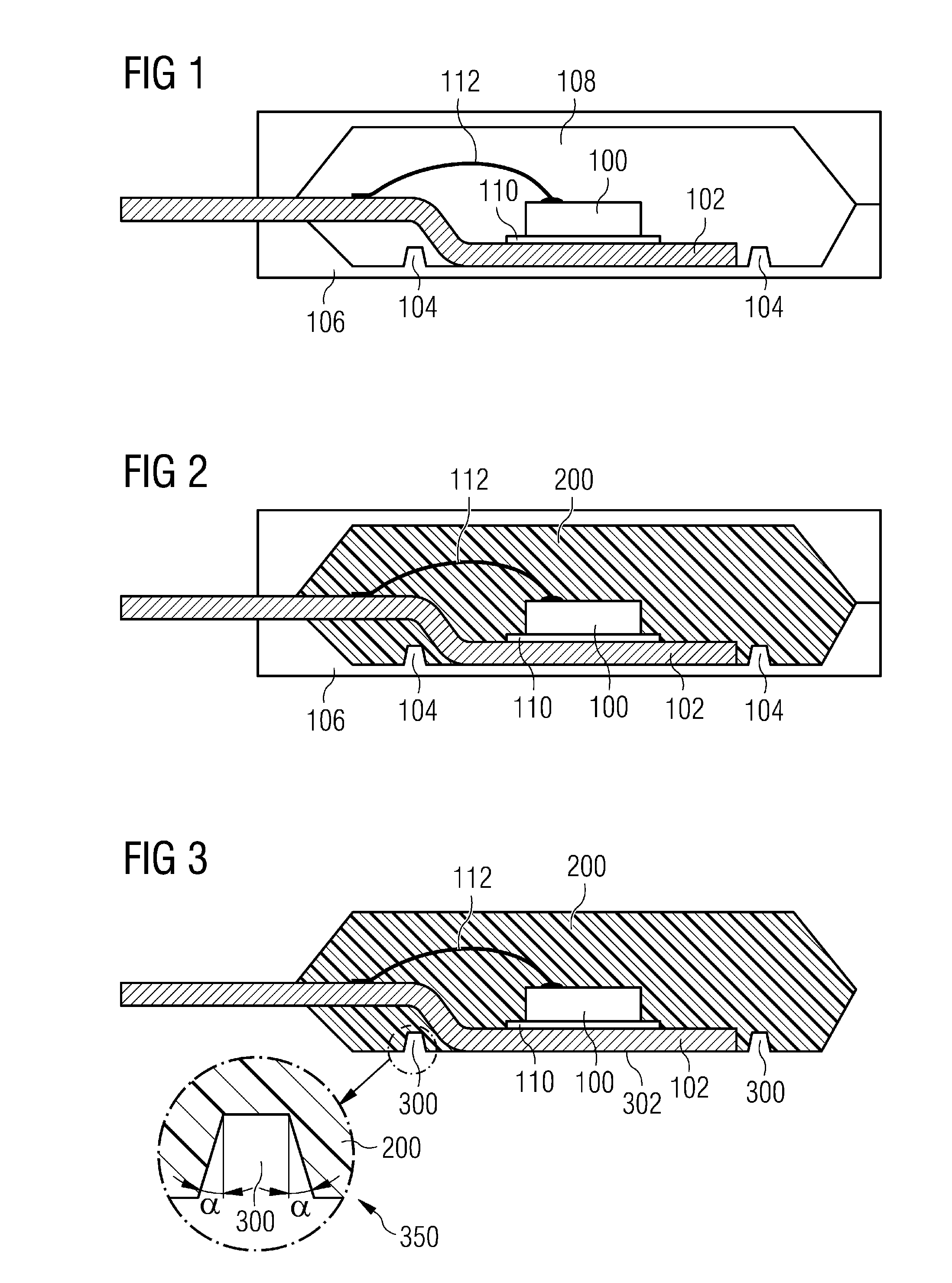
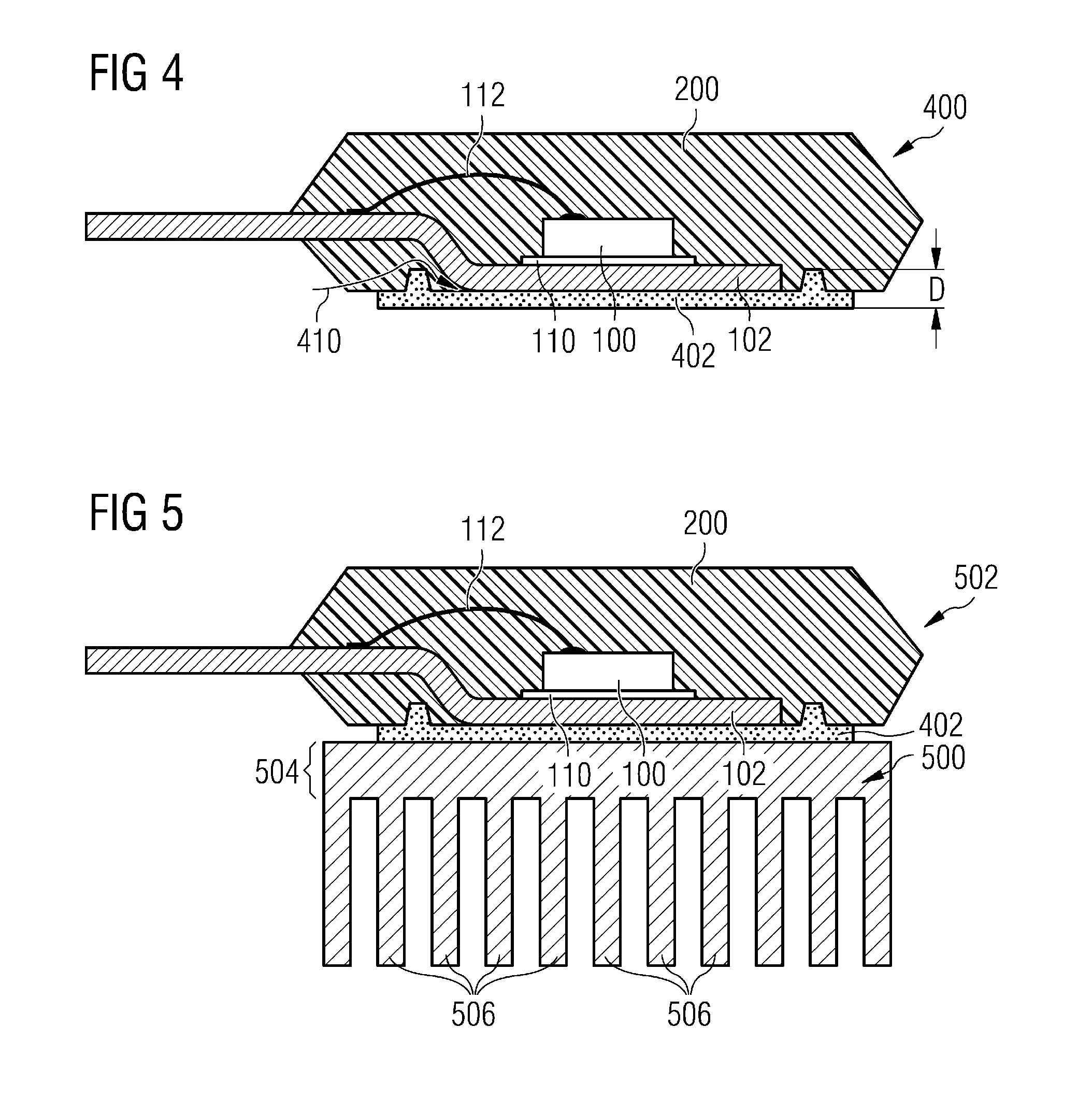
[0012]One underlying idea of the exemplary embodiments can be seen in that a peripheral well is placed in the outer area between the heat sink / chip carrier package and the compound encapsulating the component (encapsulation structure), which peripheral well is utilized by filling the same with a thermally conductive and electrically insulating compound in the form of the thermal interface structure, in order to improve the electrical insulation of a two-material component system. By placing a recess or other discontinuity in and / or on the encapsulating material or in and / or on the encapsulation structure of the electronic chip around the heat sink component or the electrical carrier or chip carrier (for example a copper lead frame), the adhesion can be improved and the path to be...


PUM


Abstract

Method for manufacturing an electronic semiconductor package, in which method an electronic chip (100) is coupled to a carrier, the electronic chip is at least partially encapsulated by means of an encapsulation structure having a discontinuity, and the carrier is partially encapsulated, and at least one part of the discontinuity and a volume connected thereto adjoining an exposed surface section of the carrier are covered by an electrically insulating thermal interface structure, which electrically decouples at least one part of the carrier with respect to its surroundings.

Description

BACKGROUND[0001]1. Field[0002]The invention relates to an electronic semiconductor package, an electronic arrangement and a method for manufacturing an electronic semiconductor package.[0003]2. Description of the State of the Art[0004]When package an electronic chip by means of an encapsulation structure, the electronic chip mounted on the electric carrier is cast with an encapsulating compound and thereby a surface region of the electrical carrier is kept free. A thermal interface structure (TIM, thermal interface material), which electrically decouples the electrical carrier with respect to its surroundings and couples it thermally with its surroundings, can then be mounted on one part of the encapsulation structure and the surface region of the electrical carrier. The user can then mount a heat dissipation element, for example in the form of a heat sink, on such an electronic semiconductor package, in order to be able to discharge accumulated waste heat from the electronic semico...

Claims


Application Information

Patent Timeline
Patent Type & Authority Applications(United States)
IPC IPC(8): H01L23/31H01L21/52H01L23/367H01L21/56
CPCH01L23/3157H01L21/56H01L21/52H01L23/3675H01L2224/32013H01L2224/32245H01L2224/48091H01L2224/48247H01L2224/48465H01L2224/73265H01L2924/1815H01L2924/1305H01L2924/13055H01L23/3107H01L23/3142H01L21/565H01L23/3737H01L23/4334H01L2924/181H01L24/48H01L2924/00014H01L2224/92247H01L2924/00H01L2924/00012H01L2224/45099H01L21/3105H01L21/4871H01L23/49551H01L24/83H01L24/85H01L24/92H01L2924/17747
Inventor FUERGUT, EDWARDMENGEL, MANFRED
Owner INFINEON TECH AG
Why Eureka
Try Eureka