
Semiconductor storage device

a technology of semiconductors and storage devices, applied in the field of semiconductor storage devices, can solve the problems of increasing power consumption, large power consumption, and large power consumption of nor-type cam cells, and achieve the effects of reducing power consumption, reducing power consumption, and increasing operation

Active Publication Date: 2015-04-23
TOHOKU UNIV
View PDF4 Cites 0 Cited by
  • Summary
  • Abstract
  • Description
  • Claims
  • Application Information

AI Technical Summary

Benefits of technology

The present invention provides a high-speed and low-power-consumption Content Addressable Memory (CAM) that can operate on a word-to-word basis. This is achieved by segmenting the search operation cycle time using a small partial delay in the initial partial word circuit, resulting in higher operation than conventional synchronous CAM. The asynchronous control method is used to achieve independent operation on the word to word basis, reducing power consumption without using pipeline registers and achieving a circuit not affected by the worst delay. The word circuit segmentation method also decreases power consumption compared to conventional methods.

Problems solved by technology

Hence, the mismatched word circuit discharges the ML capacitance in the NOR-type cell frequently, and thus consumes large power.
The NOR-type CAM cell operates at high speed but consumes large power.
Furthermore, due to increase in network traffic in recent years, the number of entries to be stored has been increased, hence the power consumption is increasing.
With this method, however, it is necessary to add a sense amplifier, etc. between segments, which causes delay to increase.

Method used


Image

  • Semiconductor storage device
  • Semiconductor storage device
  • Semiconductor storage device

Examples


Embodiment Construction

[0109]The embodiments of the present invention will hereinafter be described in detail by referring to drawings.

(Word-Overlapped Search)

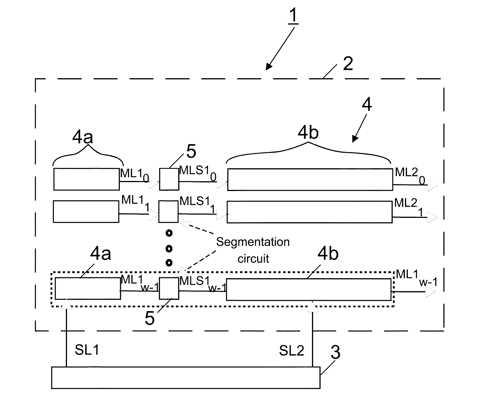
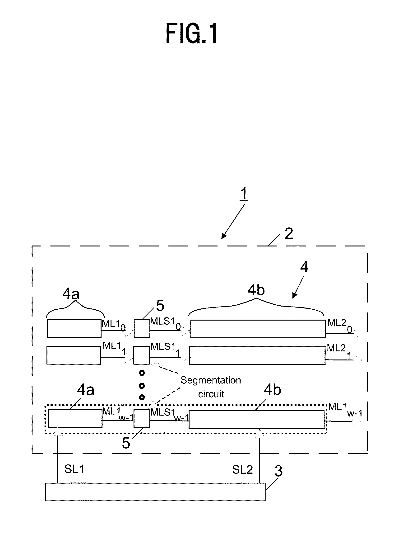
[0110]FIG. 1 is a block diagram showing a semiconductor storage device 1 adopting a word-overlapped search scheme (WOS scheme) according to the present invention.

[0111]As shown in FIG. 1, the semiconductor storage device 1 of the present invention includes: a CAM block 2; and an input controller 3. The semiconductor storage device 1 of the present invention is also called a content-addressable memory (CAM).

[0112]The CAM block 2 contains a word block (word circuit) 4 of a plurality of words (w word) for storing n-bit words, and operates based on self-control or synchronous control.

[0113]The word block 4 includes: a small k-bit sub word 4a; a segmentation circuit 5 connected to the k-bit sub word 4a; and a subsequent (n-k)-bit sub word 4b connected to the output side of the segmentation circuit 5. In other words, in the word block 4, the small k-bit s...


PUM


Abstract

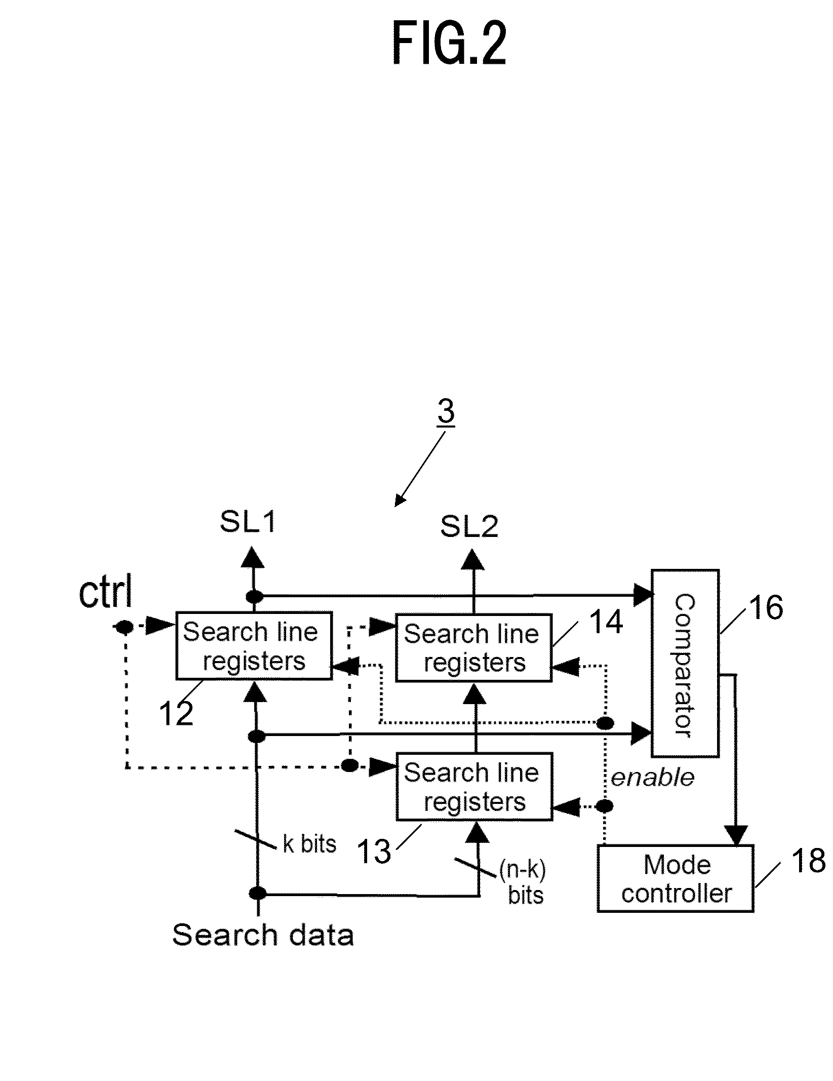
A semiconductor storage device 1 includes: an input controller (3); and a content-addressable memory block (2) connected to the input controller (3). Each word circuit (4) of the content-addressable memory block (2) includes: a k-bit 1st-stage sub word (4a) connected to search line 1 (SL1) of the input controller (3); and an (n-k)-bit 2nd-stage sub word (4b) connected to search line 2 (SL2) of the input controller (3). The k-bit 1st-stage sub word (4a) and the (n-k)-bit 2nd-stage sub word (4b) are separated by a segmentation circuit (5). When the 1st-stage sub word outputs a match signal, the match result is stored in the segmentation circuit (5), and a plurality of local match circuits within the 2nd-stage sub word (4b) are operated.

Description

TECHNICAL FIELD[0001]The present invention relates to a semiconductor storage device. More specifically, the present invention relates to the semiconductor storage device that operates at high speed while consuming low energy.BACKGROUND ART[0002]A content-addressable memory (CAM), a type of semiconductor memories, is used as a high-speed and low-power functional memory. The CAM executes the lookup-table function that compares an input search word with a table of stored words, and returns the matching word at high speed by a fully parallel equality-search manner.[0003]The CAM is used for applications such as parametric curve extraction (Non-patent Literature 1), the Hough transformation used by the feature extraction method for digital image processing and conversion (Non-patent Literature 2), the Lempel-Ziv compression, which is one of data compression algorithms (Non-patent Literature 3), the human body communication controller (Non-patent Literature 4), the periodic event generato...

Claims


Application Information

Patent Timeline
IPC IPC(8): G11C15/04
CPCG11C15/04G11C15/00
Inventor HANYU, TAKAHIROMATSUNAGA, SHOUNONIZAWA, NAOYAGAUDET, VINCENT
Owner TOHOKU UNIV
Learn More