Silicon carbide semiconductor device and method for producing the same

a technology of silicon carbide and semiconductor devices, applied in semiconductor devices, diodes, electrical devices, etc., can solve problems such as the breakage of gate insulation films, and achieve the effect of simplifying the production process

Active Publication Date: 2015-04-30
DENSO CORP +1
View PDF6 Cites 72 Cited by
  • Summary
  • Abstract
  • Description
  • Claims
  • Application Information

AI Technical Summary

Benefits of technology

[0017]As described above, the outer peripheral withstand voltage structure provided in the outer peripheral region can be made of the impurity embedded region, and the step of forming the second low concentration region and the second high concentration region pr

Problems solved by technology

Therefore, the intensity of electric field applied to the gate insulation film, when

Method used


Image

  • Silicon carbide semiconductor device and method for producing the same
  • Silicon carbide semiconductor device and method for producing the same
  • Silicon carbide semiconductor device and method for producing the same

Examples


first embodiment

[0038]A first embodiment of the present disclosure will be described. Hereinafter, an SiC semiconductor device formed with an inversion type MOSFET, as an example of a semiconductor switching element with a trench gate structure, will be described.

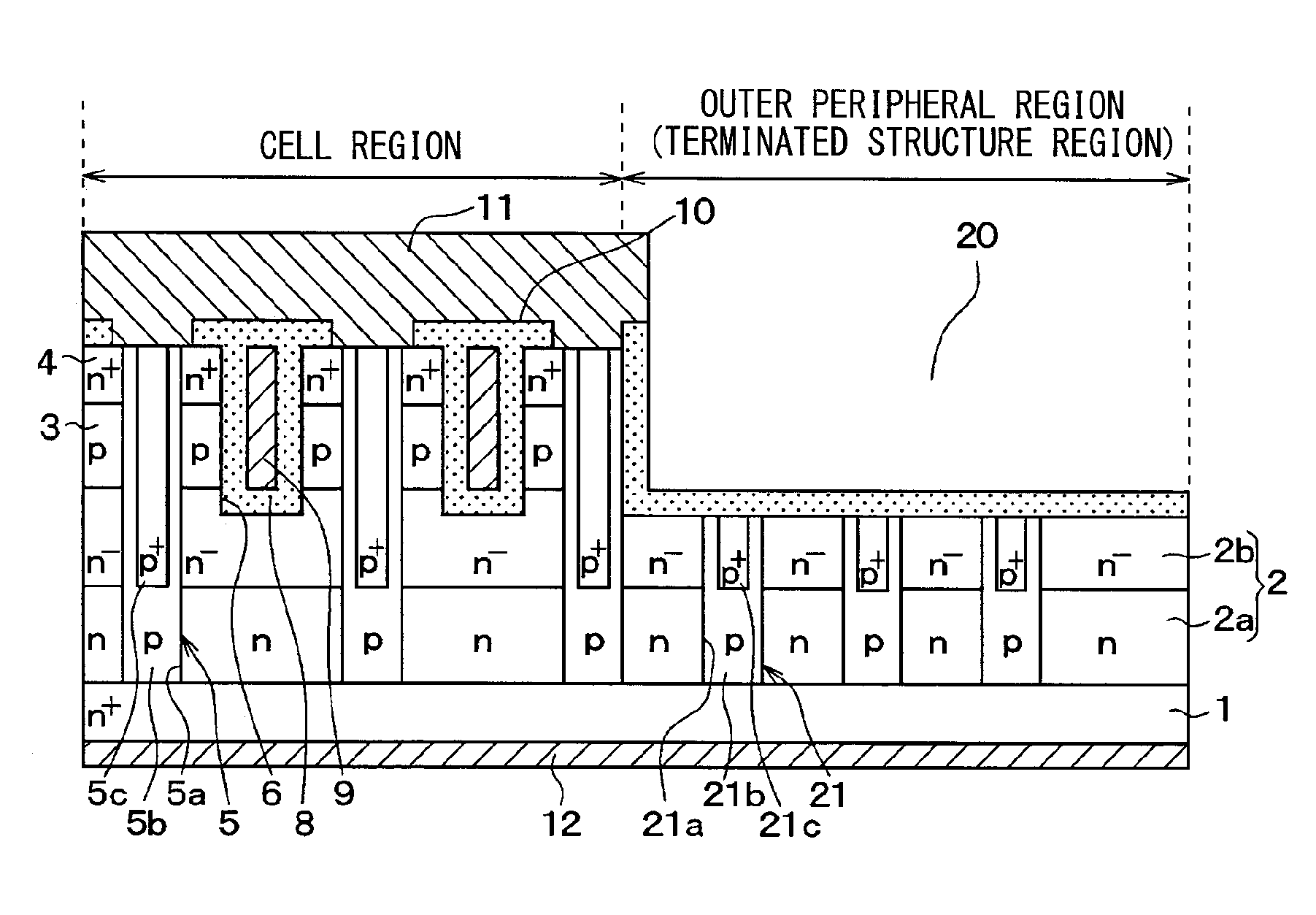
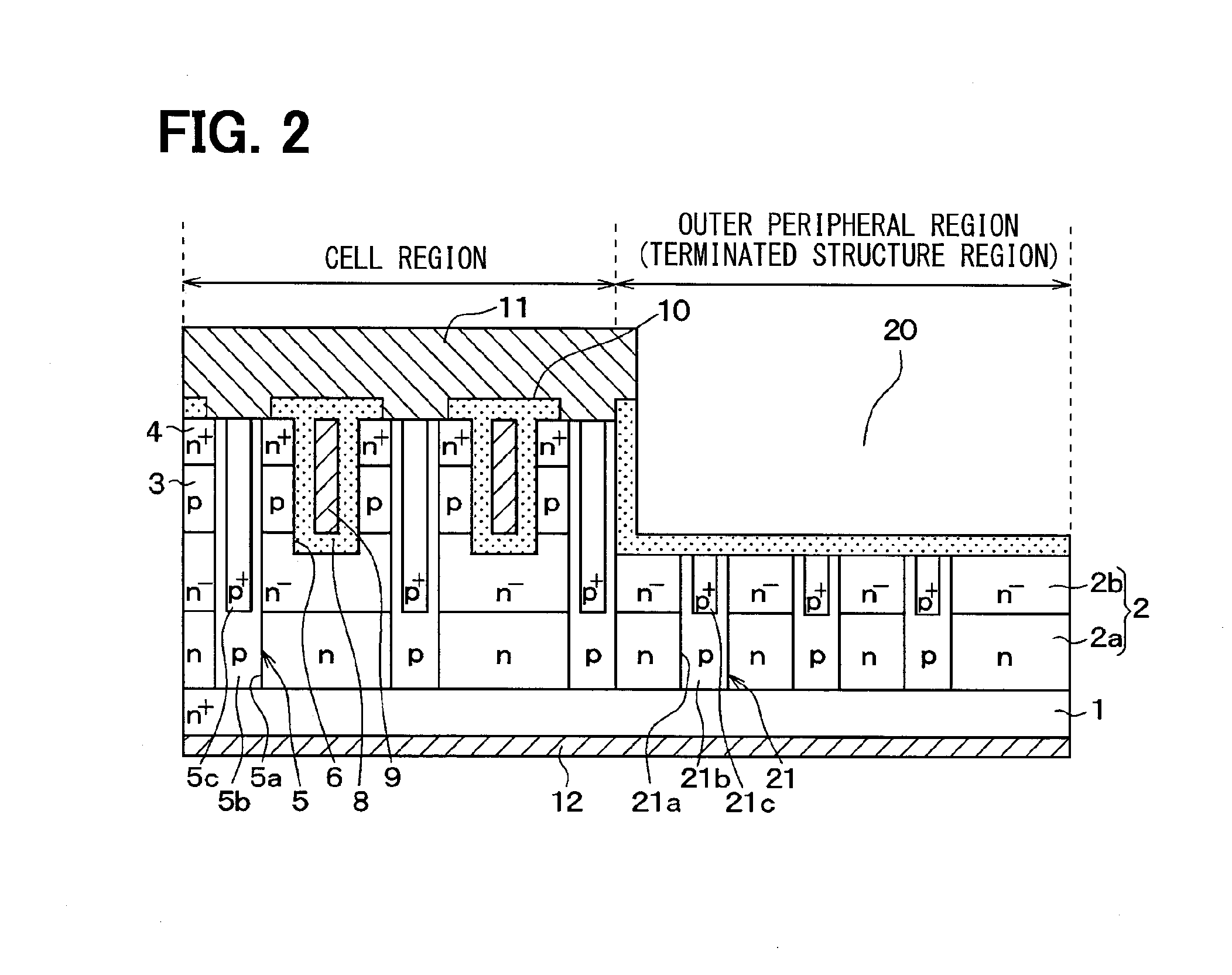
[0039]An SiC semiconductor device shown in FIG. 1 has a structure that includes a cell region in which a semiconductor element is formed, and an outer peripheral region (terminated structure region) in which an outer peripheral withstand voltage structure surrounding the cell region is provided.

[0040]In the present embodiment, as the semiconductor element, the MOSFET with the inversion type trench gate structure is provided.

[0041]As shown in FIG. 2, the SiC semiconductor device is formed using a semiconductor substrate in which an n− type drift layer 2, a p type base region 3, and an n+ type source region 4, which are made of SiC, are subsequently epitaxially grown on a main surface of an n+ type substrate 1 made of SiC.

[0042]The n+ type s...

second embodiment

[0077]A second embodiment of the present disclosure will be described. The present embodiment is different from the first embodiment in regard to the depth of the trench 6 and the recessed portion 20. The others are similar to those of the first embodiment. Therefore, only a part different from the first embodiment will be described.

[0078]In the present embodiment, as shown in FIG. 4, the trench 6 and the recessed portion 20 are different in depth. In particular, the recessed portion 20 is deeper than the trench 6. In the case where the trench 6 and the recessed portion 20 are set to have different depths, it is possible to design the withstand voltage for each of the trench 6 and the recessed portion 20. It is possible to suitably adjust the withstand voltage such that breakdown is generated in the outer peripheral region, for example.

[0079]In the production process of the SiC semiconductor device having such a structure, the step of forming the trench 6 and the step of forming the...

third embodiment

[0080]A third embodiment of the present disclosure will be described. In the present embodiment, a structure of the p type impurity embedded layer 21 is modified from that of the first embodiment, and the others are the similar to those of the first embodiment. Therefore, only a part different from the first embodiment will be described.

[0081]In the present embodiment, as shown in FIG. 5, the depth of the trenches 21a and the p type impurity embedded layers 21 is varied. The depth of the trenches 21a and the p type impurity embedded layers 21 is gradually reduced as a function of distance from the cell region in an outward direction. In this way, the depth of the p type impurity embedded layers 21 is gradually varied. Therefore, it is possible to configure the p type impurity embedded layers 21 with the shape according to an equipotential line distribution in the outer peripheral region, and thus it is possible to reduce the region necessary for a termination structure. For this rea...


PUM


Abstract

An SiC semiconductor device has a p type region including a low concentration region and a high concentration region filled in a trench formed in a cell region. A p type column is provided by the low concentration region, and a p+ type deep layer is provided by the high concentration region. Thus, since a SJ structure can be made by the p type column and the n type column provided by the n type drift layer, an on-state resistance can be reduced. As a drain potential can be blocked by the p+ type deep layer, at turnoff, an electric field applied to the gate insulation film can be alleviated and thus breakage of the gate insulation film can be restricted. Therefore, the SiC semiconductor device can realize the reduction of the on-state resistance and the restriction of breakage of the gate insulation film.

Description

CROSS REFERENCE TO RELATED APPLICATIONS[0001]This application is based on Japanese Patent Applications No. 2012-134031 filed on Jun. 13, 2012 and No. 2013-49229 filed on Mar. 12, 2013, the disclosures of which are incorporated herein by reference.TECHNICAL FIELD[0002]The present disclosure relates to a silicon carbide (hereinafter referred to as SiC) semiconductor device having a switching element with a trench gate structure, and a method for producing the same.BACKGROUND ART[0003]Conventionally, a patent literature 1 has proposed an SiC semiconductor device that aims to restrict breakage of a gate insulation film in a MOSFET with a trench gate structure and to improve surge withstand (avalanche resistance) of the element. Specifically, a p+ type deep layer is provided to a position lower than the bottom surface of the trench, between trench gate structures, and is further deepened at a middle of a cell region. By forming the p+ type layer in this manner, concentration of an electr...

Claims


Application Information

Patent Timeline
IPC IPC(8): H01L29/78H01L29/06H01L21/308H01L29/10H01L21/04H01L21/306H01L29/66H01L29/16
CPCH01L29/7811H01L29/7806H01L29/7813H01L29/66734H01L29/66068H01L21/308H01L29/0696H01L29/1608H01L29/1095H01L21/0475H01L21/30604H01L29/0634H01L21/8213H01L29/0615H01L29/063H01L29/0661H01L29/0878H01L29/41766H01L29/66727H01L29/861H01L29/872H01L21/046H01L29/4236H01L29/16H01L29/78Y10S438/974H01L21/761H01L29/157H01L29/158
Inventor TAKEUCHI, YUICHISUZUKI, NAOHIROSUGIMOTO, MASAHIROTAKAYA, HIDEFUMISOENO, AKITAKAMORIMOTO, JUNSOEJIMA, NARUMASAWATANABE, YUKIHIKO
Owner DENSO CORP
Why Eureka
Try Eureka