Programmable logic circuit architecture using resistive memory elements

a technology of resistive memory elements and logic circuits, applied in logic circuits using specific components, pulse techniques, instruments, etc., can solve the problems of high overhead of programming circuits, undermine the benefit brought by replacement, and not solve the problem of extensive fabrication of routing buffers

Active Publication Date: 2015-05-07
RGT UNIV OF CALIFORNIA
View PDF8 Cites 16 Cited by
  • Summary
  • Abstract
  • Description
  • Claims
  • Application Information

AI Technical Summary

Benefits of technology

[0018]Further introduction of three-dimensional (3D) technologies provides more improvement.

Problems solved by technology

However, this direct replacement leads to high overhead of programming circuits for resistive memory elements, which undermines the benefit brought by the replacement.
Also, the method in [1] does not solve the problem of extensive fabrication of routing buffers.
The method in [2] leads to speed degradation and high power consumption due to large capacitance of nanowires.

Method used


Image

  • Programmable logic circuit architecture using resistive memory elements
  • Programmable logic circuit architecture using resistive memory elements
  • Programmable logic circuit architecture using resistive memory elements

Examples


Embodiment Construction

[0026]In the following description of the preferred embodiment, reference is made to the accompanying drawings which form a part hereof, and in which is shown by way of illustration a specific embodiment in which the invention may be practiced. It is to be understood that other embodiments may be utilized and structural changes may be made without departing from the scope of the present invention.

[0027]Overview

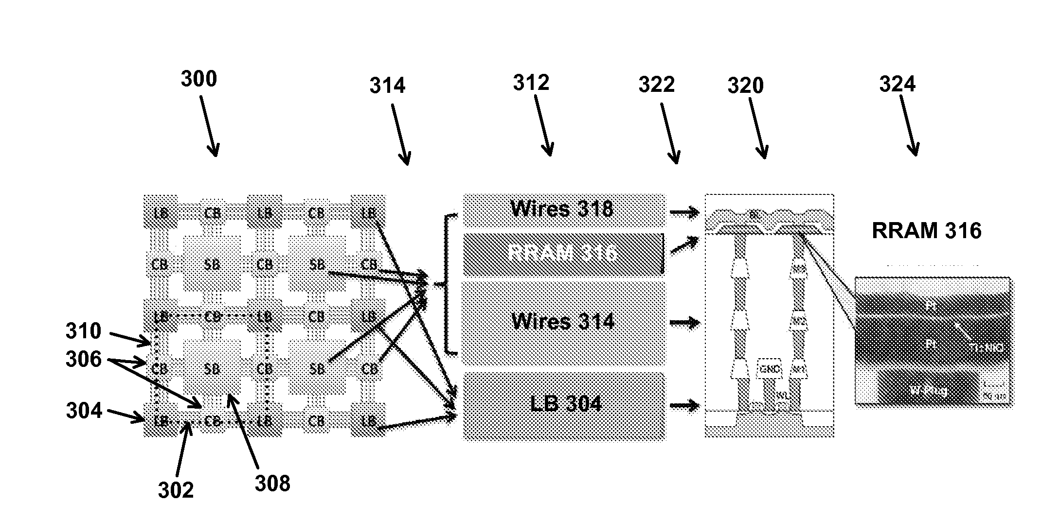
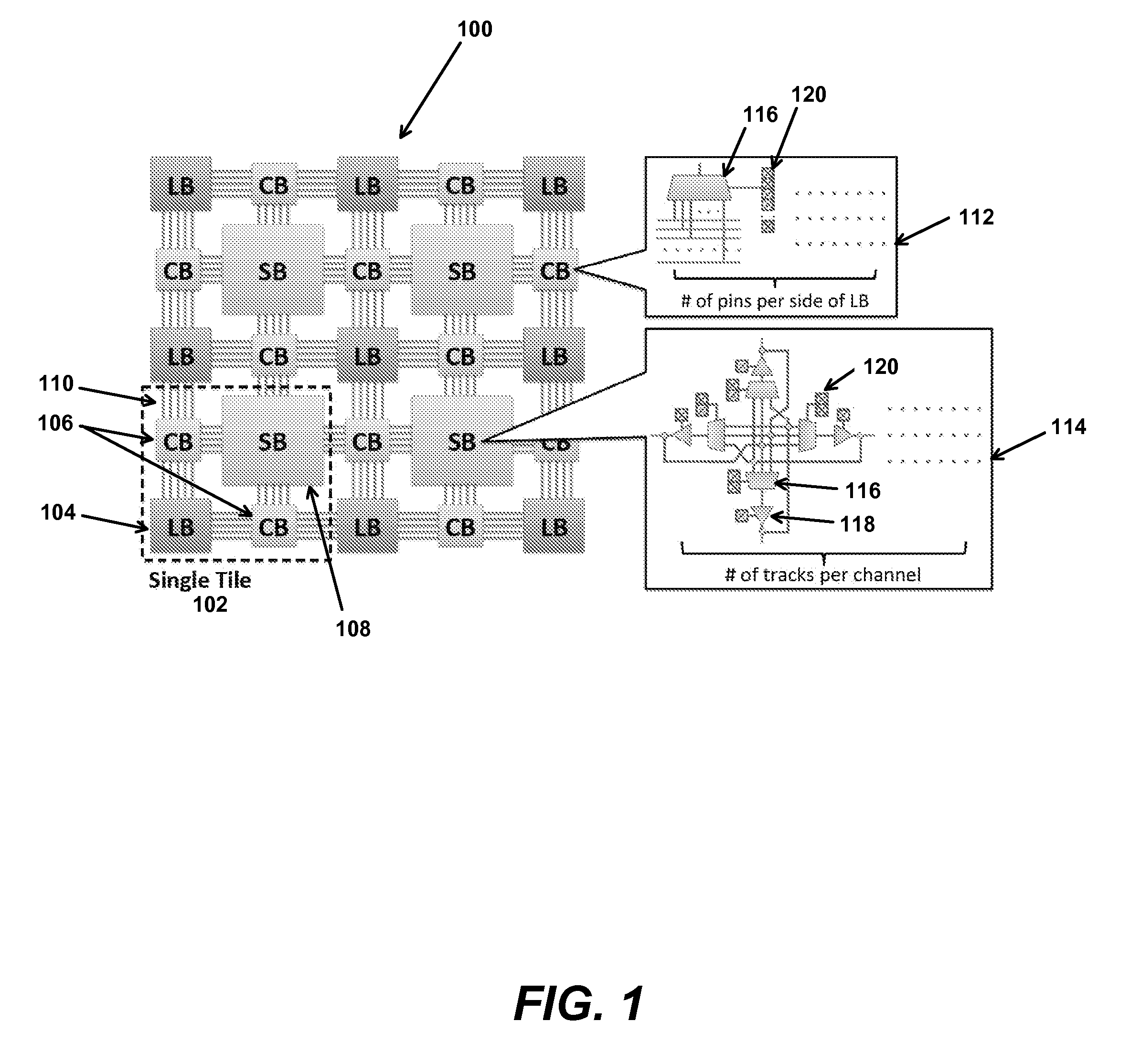
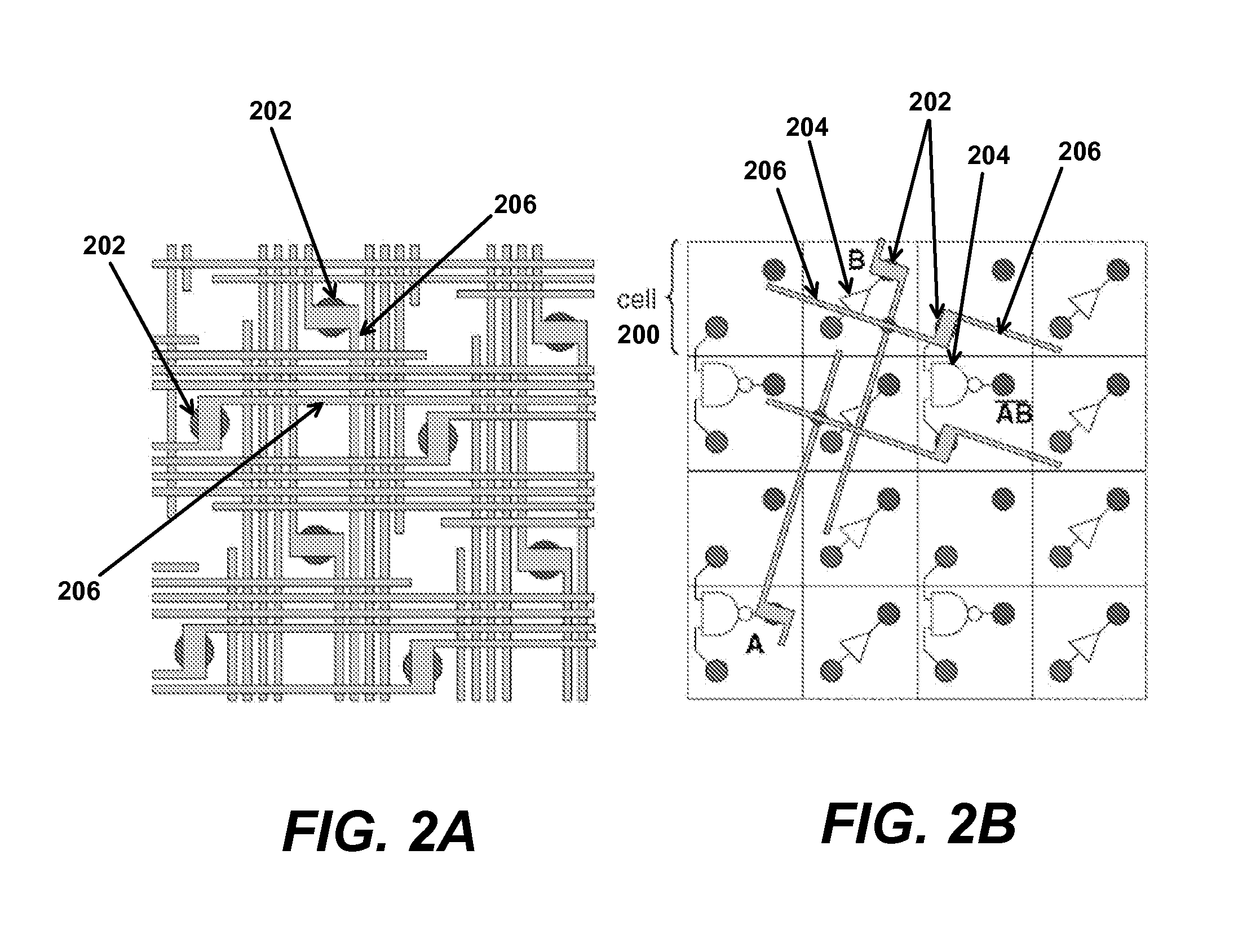
[0028]The present invention redesigns FPGA programmable interconnects based on resistive memory elements, known as resistive random access memory (RRAM) or memristors.

[0029]Compared to [1], this invention has the following advantages:

[0030]1. This invention better fits the fabrication structure of resistive memory elements. The integration of SRAM cells in programmable interconnects were optimized for conventional FPGAs. One SRAM cell usually involves a CMOS layer and multiple metal layers. In contrast, a resistive memory element does not involve a CMOS layer and, in most case...


PUM


Abstract

A programmable logic circuit architecture using resistive memory elements. The proposed circuit architecture uses the conventional island-based Field Programmable Gate Array (FPGA) architecture, but with novel integration of CMOS-compatible resistive memory elements that can be programmed efficiently. In the proposed architecture, the programmable interconnects of FPGA are redesigned to use only resistive memory elements and metal wires. Then, the interconnects can be entirely fabricated over logic blocks to save area while keeping their architectural functions unchanged, and the programming transistors can be shared among resistive memory elements to save area. Finally, on-demand buffer insertion is proposed as the buffering solution to achieve more speedup.

Description

CROSS REFERENCE TO RELATED APPLICATION[0001]This application claims the benefit under 35 U.S.C. Section 119(e) of co-pending and commonly-assigned U.S. Provisional Patent Application Ser. No. 61 / 654,542, filed on Jun. 1, 2012, by Jingsheng J. Cong and Bingjun Xiao, entitled “PROGRAMMABLE LOGIC CIRCUIT ARCHITECTURE USING RESISTIVE MEMORY ELEMENTS,” attorneys' docket number 30435.257-US-P1 (2012-038-1), which application is incorporated by reference herein.BACKGROUND OF THE INVENTION[0002]1. Field of the Invention[0003]This invention is related to programmable logic circuits, and more specifically, to a programmable logic circuit architecture using resistive memory elements.[0004]2. Description of the Related Art[0005](Note: This application references a number of different publications as indicated throughout the specification by one or more reference numbers within brackets, e.g., [x]. A list of these different publications ordered according to these reference numbers can be found b...

Claims


Application Information

Patent Timeline
Patent Type & Authority Applications(United States)
IPC IPC(8): H03K19/177G11C13/00G11C5/06H01L45/00
CPCH03K19/1776G11C5/06G11C13/0002H01L45/16H03K19/1736H03K19/17736H10N70/011
Inventor CONG, JINGSHENG J.XIAO, BINGJUN
Owner RGT UNIV OF CALIFORNIA
Why Eureka
Try Eureka