Manufacture of semiconductor device having insulation film of high dielectric constant

a technology of dielectric constant and insulation film, which is applied in the direction of coating, transistor, chemical vapor deposition coating, etc., can solve the problems of gate leak current becoming uncontrollable, boron penetration in the p-channel transistor is of problem, and the threshold voltage of the transistor is reduced, so as to achieve enhanced nitrogen in the introduction of

Inactive Publication Date: 2005-08-04
FUJITSU LTD
View PDF13 Cites 11 Cited by
  • Summary
  • Abstract
  • Description
  • Claims
  • Application Information

AI Technical Summary

Benefits of technology

[0016] According to one aspect of the invention, there is provided a method of manufacturing a semiconductor device comprising the steps of: (a) heating a silicon substrate in a reaction chamber; and (b) depositing an insulating film having a specific dielectric constant higher than that of silicon oxide on said heated silicon substrate by thermal CVD, by supplying film-forming gas containing source gas, nitridizing gas, and nitridation enhancing gas to a surface of said heated silicon substrate.
[0017] According to another aspect of the invention, there is provided a semiconductor device comprising: a silicon substrate having an active region; a gate insulation film formed on a surface of the active region of the silicon substrate, and including a high-dielectric-constant insulation film essentially consisting of oxide of Hf1-xAlx (0<x<0.3), which includes N of at least 0.5 at %, and has a specific dielectric constant higher than that of silicon oxide; a gate electrode formed on the gate insulation film and including an impurity-doped silicon layer; and source / drain regions formed on both sides of the gate electrode by doping impurity in the active region of the silicon substrate.
[0018] It is not always easy to introduce nitrogen into metal oxide. Introduction of nitrogen is enhanced by CVD using a nitridizing gas and nitridation enhancing gas. As nitridizing gas, it is preferable to use at least one of ammonia, bis-tertial-butyl amino silane (BTBAS), and tri-ethyl amine (TEN). As nitridation enhancing gas, it is preferable to use a gas comprising hydrogen.

Problems solved by technology

When the impurity in the gate electrode diffuses into the channel region, it lowers the threshold voltage of the transistor, and causes punch-through.
Especially, the penetration of boron in the p-channel transistor is of problem.
With that film thickness, the tunnel current starts flowing, the gate leak current becomes uncontrollable, and an increase in power dissipation cannot be avoided.
The use of a new material having a high specific dielectric constant for the gate insulation film of an IG-FET brings about a new problem.

Method used


Image

  • Manufacture of semiconductor device having insulation film of high dielectric constant
  • Manufacture of semiconductor device having insulation film of high dielectric constant
  • Manufacture of semiconductor device having insulation film of high dielectric constant

Examples


Embodiment Construction

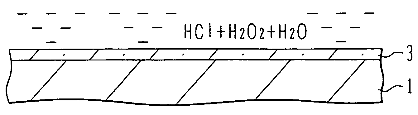
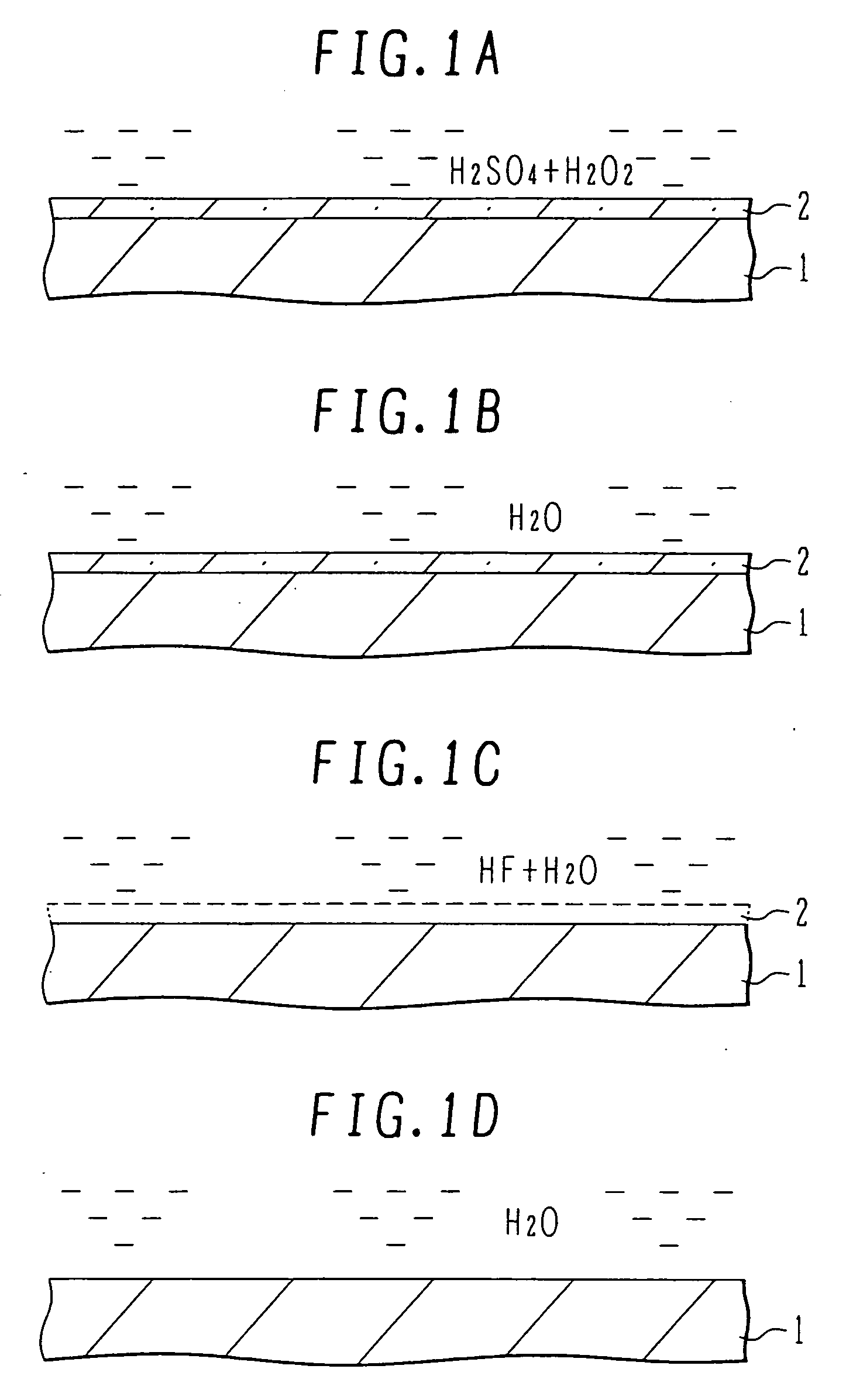
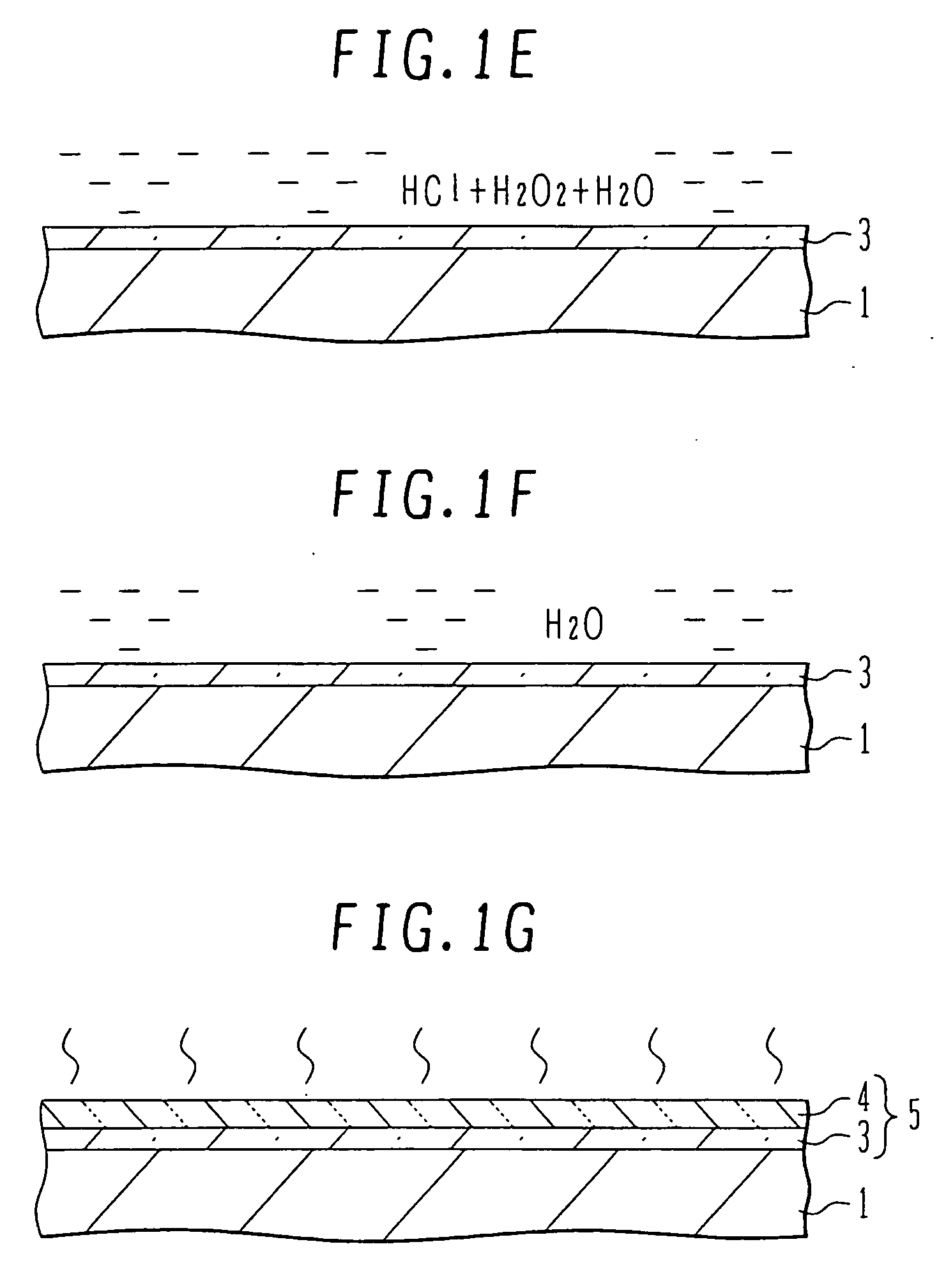
[0025] Hafnium oxide is an insulator which can provide a specific dielectric constant several to ten and several times as large as the specific dielectric constant of silicon oxide, and has a high potential as the gate insulation film of an IG-FET. Hafnium oxide (hafnia) is easily crystallized, and it is not easy to form a dense film of a thin and uniform thickness. When a gate insulation film is made of hafnium oxide only on a silicon substrate, a crystalline insulation film with a large leak current is likely to be formed.

[0026] The crystallization can be suppressed by mixing aluminum oxide (alumina) (Al2O3) in the hafnium oxide (HfO2). The suppressed crystallization reduces the leak current. The aluminum oxide has a specific dielectric constant lower than that of the hafnium oxide. To acquire a specific dielectric constant as high as possible, it is preferable that the amount of the aluminum oxide to be mixed in the hafnium oxide should be limited to Hf1-xAlxO (01-xAlxO (0.1


PUM

PropertyMeasurementUnit
thicknessaaaaaaaaaa
temperatureaaaaaaaaaa
pressureaaaaaaaaaa

Abstract

A method contains the steps of (a) heating a silicon substrate in a reaction chamber; and (b) supplying film-forming gas containing source gas, nitridizing gas, and nitridation enhancing gas to a surface of the heated silicon substrate, to deposit on the silicon substrate an Hf1-xAlxO:N film (0.1<x<0.3) having a higher specific dielectric constant than that of silicon oxide, and incorporating N, by thermal CVD. The method can form an oxide film of Hf1-xAlxO (0<x<0.3) having desired characteristics, as a gate insulation film.

Description

CROSS REFERENCE TO RELATED APPLICATION [0001] This application is a continuation application of International Patent Application No. PCT / JP03 / 03198, filed on Mar. 17, 2003, the entire contents of which are incorporated herein by reference.BACKGROUND OF THE INVENTION [0002] A) Field of the Invention [0003] The present invention relates to a semiconductor device and a method of manufacturing a semiconductor device, and, more particularly, to a semiconductor device having an insulation film of a high dielectric constant and a method of manufacturing the semiconductor device. B) Description of the Related Art [0004] Insulated gate (IG) field effect transistors (FETs), typical examples of which are MOS transistors, are widely used as typical semiconductor devices used in a semiconductor integrated circuit device. For a larger scale integration of semiconductor integrated circuit devices, IG-FETs have been miniaturized according the scaling law. Miniaturization reduces the sizes of IG-FE...

Claims


Application Information

Patent Timeline
Patent Type & Authority Applications(United States)
IPC IPC(8): C23C16/30H01L21/28H01L21/314H01L21/316H01L21/318H01L21/336H01L29/51H01L29/78
CPCC23C16/308H01L21/28167H01L21/28194H01L21/28202H01L21/3141H01L21/3143H01L29/6659H01L21/3145H01L21/31616H01L21/31645H01L29/513H01L29/517H01L29/518H01L21/3144H01L21/02178H01L21/02271H01L21/02211H01L21/02164H01L21/02181H01L21/02194H01L21/022
Inventor YAMAGUCHI, MASAOMI
Owner FUJITSU LTD
Why Eureka
Try Eureka