Method for producing m-plane nitride-based light-emitting diode

a technology of nitride-based light-emitting diodes and m-planes, which is applied in the direction of semiconductor/solid-state device manufacturing, electrical apparatus, semiconductor devices, etc., can solve the problems of insufficient research on m-plane nitride-based leds, and achieve the effect of reducing the power consumption of illuminators or display devices

Inactive Publication Date: 2015-05-07
MITSUBISHI CHEM CORP +1
View PDF4 Cites 8 Cited by
  • Summary
  • Abstract
  • Description
  • Claims
  • Application Information

AI Technical Summary

Benefits of technology

[0011]For reducing the power consumption of illuminators or display devices which employ LEDs, it is important to reduce the forward voltage (i.e., operating voltage) of the LEDs. It is expected that almost all of the incandescent light bulbs and fluorescent lamps will be replaced with LED illuminators in the near feature. In that case, only a 0.1-V difference in the forward voltage of each LED greatly affects the amount of electric power to be consumed by the whole society.

Problems solved by technology

Similar investigations on m-plane nitride-based LEDs have not been sufficiently made yet.

Method used


Image

  • Method for producing m-plane nitride-based light-emitting diode
  • Method for producing m-plane nitride-based light-emitting diode
  • Method for producing m-plane nitride-based light-emitting diode

Examples


Embodiment Construction

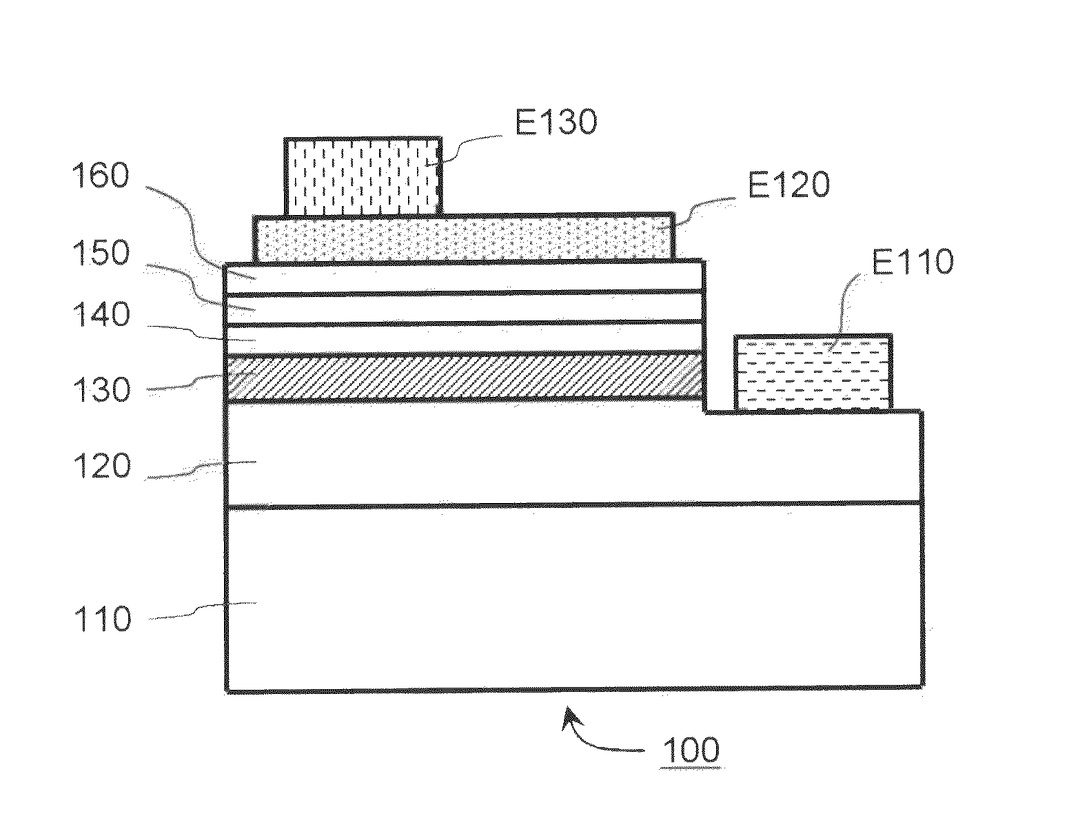
[0042]In this description, the term “InGaN” means a mixed crystal of InN and GaN, and “AlGaN” means a mixed crystal of AlN and GaN. Furthermore, the term “InAlGaN” means a mixed crystal of InN, AlN, and GaN.

[0043]In this description, an off-angled m-plane GaN substrate is often referred to. The off-angle of an m-plane GaN substrate, as shown in FIG. 11, is the angle φ between [10-10] and the normal vector to the main growth surface (main surface used for epitaxial growth) of the substrate. The +c-direction off-angle φc of the m-plane GaN substrate is the angle φc between [10-10] and the projection obtained by projecting the normal vector to the main growth surface on the a-plane (plane orthogonal to [11-20]). In cases when the projection has a [0001] component (+c component), the value of φc is plus. In contrast, in cases when the projection has a [000-1] component (−c component), the value of φc is minus.

[0044]The method for producing an m-plane nitride-based light-emitting diode a...


PUM

PropertyMeasurementUnit
thicknessaaaaaaaaaa
thicknessaaaaaaaaaa
thicknessaaaaaaaaaa

Abstract

Provided is a novel method for producing an m-plane nitride-based LED, the method making it possible to obtain an m-plane nitride-based LED reduced in forward voltage. The method comprising (i) a step of forming an active layer consisting of a nitride semiconductor over an n-type nitride semiconductor layer in which an angle between the thickness direction and the m-axis of a hexagonal crystal is 10 degrees or less, (ii) a step of forming an AlGaN layer doped with a p-type impurity over the active layer, (iii) a step of forming a contact layer consisting of InGaN is formed on the surface of the AlGaN layer, and (iv) a step of forming an electrode on the surface of the contact layer.

Description

CROSS-REFERENCE TO RELATED APPLICATION[0001]This is a continuation of International Application PCT / JP2013 / 067267, filed on Jun. 24, 2013, and designated the U.S., (and claims priority from Japanese Patent Application 2012-141778 which was filed on Jun. 25, 2012, Japanese Patent Application 2012-177193 which was filed on Aug. 9, 2012 and Japanese Patent Application 2013-048240 which was filed on Mar. 11, 2013,) the entire contents of which are incorporated herein by reference.TECHNICAL FIELD[0002]The present invention relates to a nitride-based light-emitting diode (nitride-based LED) which has a light-emitting structure formed of nitride semiconductors. Nitride semiconductors are also called nitride-based Group III-V element compound semiconductors, gallium nitride (GaN)-based semiconductors, or the like, and are compound semiconductors represented by the general formula AlxGayIn1-x-yN (0≦x≦1, 0≦y≦1, and 0≦x+y≦1), (Al,Ga,In)N, or the like. It is known that the semiconductors have a...

Claims


Application Information

Patent Timeline
Patent Type & Authority Applications(United States)
IPC IPC(8): H01L33/00H01L33/14H01L33/42
CPCH01L33/0075H01L33/42H01L2933/0016H01L2933/0066H01L33/145H01L21/02458H01L21/0254H01L21/02609H01L21/0262H01L33/007H01L33/16
Inventor KURIHARA, KAORITAKESHITA, YUTAROSHIMOYAMA, KENJITAKAI, SHINJI
Owner MITSUBISHI CHEM CORP
Why Eureka
Try Eureka