Nonvolatile memory system

a memory system and non-volatile technology, applied in the field of semiconductor memory systems, can solve the problems of conventional techniques having fundamental limits, degrading the overall performance of nand flash memory devices, etc., and achieve the effect of accurate knowledge (or efficient control of garbage collection operations) and high speed

Inactive Publication Date: 2015-05-07
THE AIO
View PDF3 Cites 42 Cited by
  • Summary
  • Abstract
  • Description
  • Claims
  • Application Information

AI Technical Summary

Benefits of technology

[0020]Therefore, a non-volatile memory system according to example embodiments may enable a host device to accurately know (or, recognize) internal operation information of a NAND flash memory device and to efficiently control a garbage collection operation that is performed by the NAND flash memory device by including a first flash translation layer, which performs the garbage collection operation, in the NAND flash memory device and by including a file system and a second flash translation layer, which controls an operation of the NAND flash memory device by interacting with the file system, in the host device. As a result, the non-volatile memory system may perform a random write operation at high speed, and may minimize (or, reduce) power consumption due to unnecessary data transfer.

Problems solved by technology

However, since the NAND flash memory device cannot perform an overwrite operation unlike a Hard-Disk Drive (HDD), the NAND flash memory device updates data by programming an update page in a log block associated with a data block and by performing an address-mapping related thereto.
However, the garbage collection operation results in time delay, additional data transfer, etc, so that overall performance of the NAND flash memory device may be degraded by the garbage collection operation.
For this reason, many studies for efficiently performing the garbage collection operation for the NAND flash memory device have been actively carried out, conventional techniques have fundamental limits because the conventional techniques mostly depend on only the FTL to perform the garbage collection operation.

Method used


Image

  • Nonvolatile memory system
  • Nonvolatile memory system
  • Nonvolatile memory system

Examples


Embodiment Construction

[0029]Hereinafter, embodiments of the present inventive concept will be explained in detail with reference to the accompanying drawings.

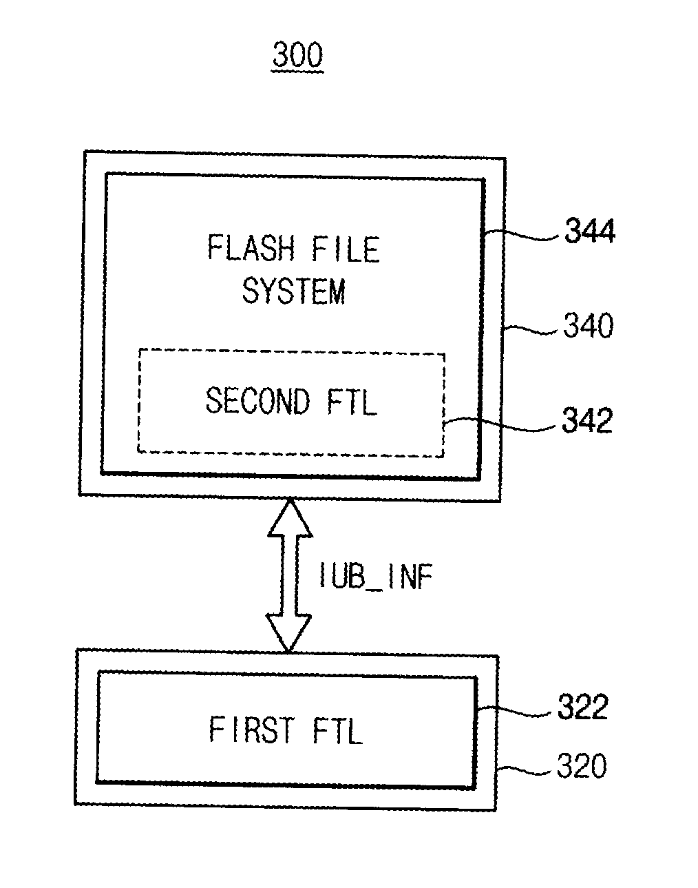
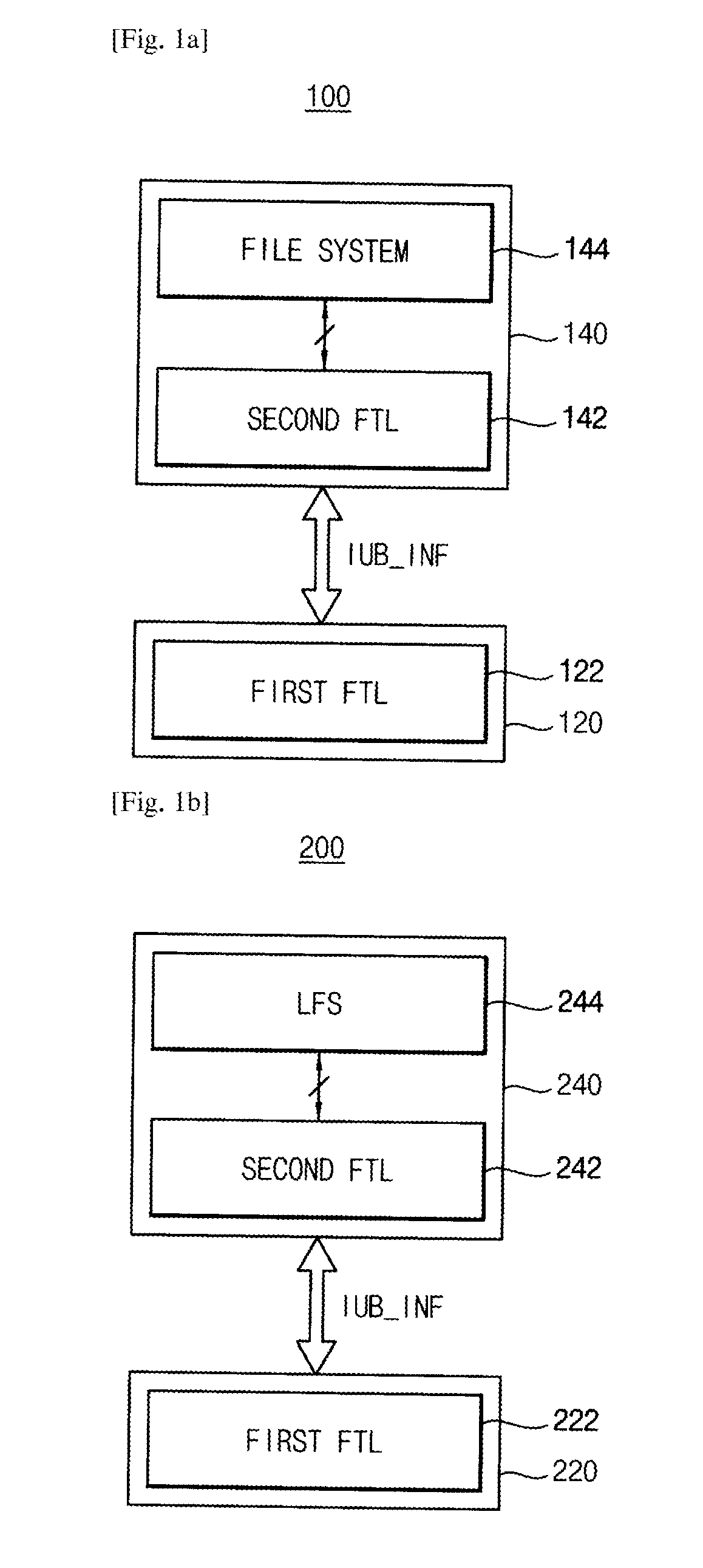
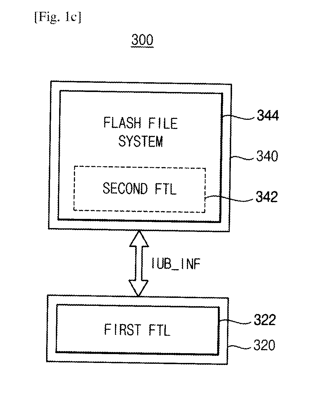
[0030]FIGS. 1A through 1C are block diagrams illustrating a non-volatile memory system according to example embodiments. For convenience of description, a non-volatile memory system according to example embodiments will be described focusing on the non-volatile memory system 100 of FIG. 1A.

[0031]Referring to FIG. 1A, the non-volatile memory system 100 may include a NAND flash memory device 120 and a host device 140. As illustrated in FIG. 1A, in the non-volatile memory system 100, a flash translation layer that controls an operation of the NAND flash memory device 120 may be divided into a first flash translation layer 122 and a second flash translation layer 142. Here, the first flash translation layer 122 may be included in the NAND flash memory device 120, and the second flash translation layer 142 may be included in the host device 140. Although...


PUM


Abstract

A non-volatile memory system includes a NAND flash memory device including a first flash translation layer that performs a garbage collection operation, and a host device including a file system and a second flash translation layer that controls an operation of the NAND flash memory device by interacting with the file system. Here, the host device provides application data in an in-ordered form to the NAND flash memory device. Thus, the non-volatile memory system can perform a random write operation at high speed, and can minimize power consumption due to unnecessary data transfer.

Description

CROSS-REFERENCE TO RELATED APPLICATION(S)[0001]This application claims priority under 35 USC §119 to Korean Patent Application No. 10-2012-0047076, filed on May 3, 2012 in the Korean Intellectual Property Office (KIPO), the contents of which are incorporated herein in its entirety by reference.BACKGROUND[0002]1. Technical Field[0003]Example embodiments relate generally to a semiconductor memory system. More particularly, embodiments of the present inventive concept relate to a non-volatile memory system including a NAND flash memory device.[0004]2. Description of the Related Art[0005]Generally, a semiconductor memory device may be classified into two types (i.e., a volatile memory device and a non-volatile memory device) according to whether data can be retained when power is not supplied. Recently, a NAND flash memory device is widely used as the non-volatile memory device because the NAND flash memory device can be made smaller while having higher capacity. However, since the NAND...

Claims


Application Information

Patent Timeline
Patent Type & Authority Applications(United States)
IPC IPC(8): G06F12/02
CPCG06F12/0253G06F2212/7211G06F2212/7205G06F12/0246G06F2212/7201Y02D10/00G11C16/06G06F12/00
Inventor HWANG, SUN-MO
Owner THE AIO
Why Eureka
Try Eureka