Lead-free solder, solder paste and semiconductor device

Active Publication Date: 2015-06-04
MK ELECTRON +4
View PDF8 Cites 2 Cited by
  • Summary
  • Abstract
  • Description
  • Claims
  • Application Information

AI Technical Summary

Benefits of technology

[0008]One or more exemplary embodiments include a lead-free solder that is environ

Problems solved by technology

However, since the ternary system is weak to oxidation and has low spreadability and low wettability, workability is poor and resistance to impact is low.
Also, the

Method used


Image

  • Lead-free solder, solder paste and semiconductor device
  • Lead-free solder, solder paste and semiconductor device
  • Lead-free solder, solder paste and semiconductor device

Examples


Embodiment Construction

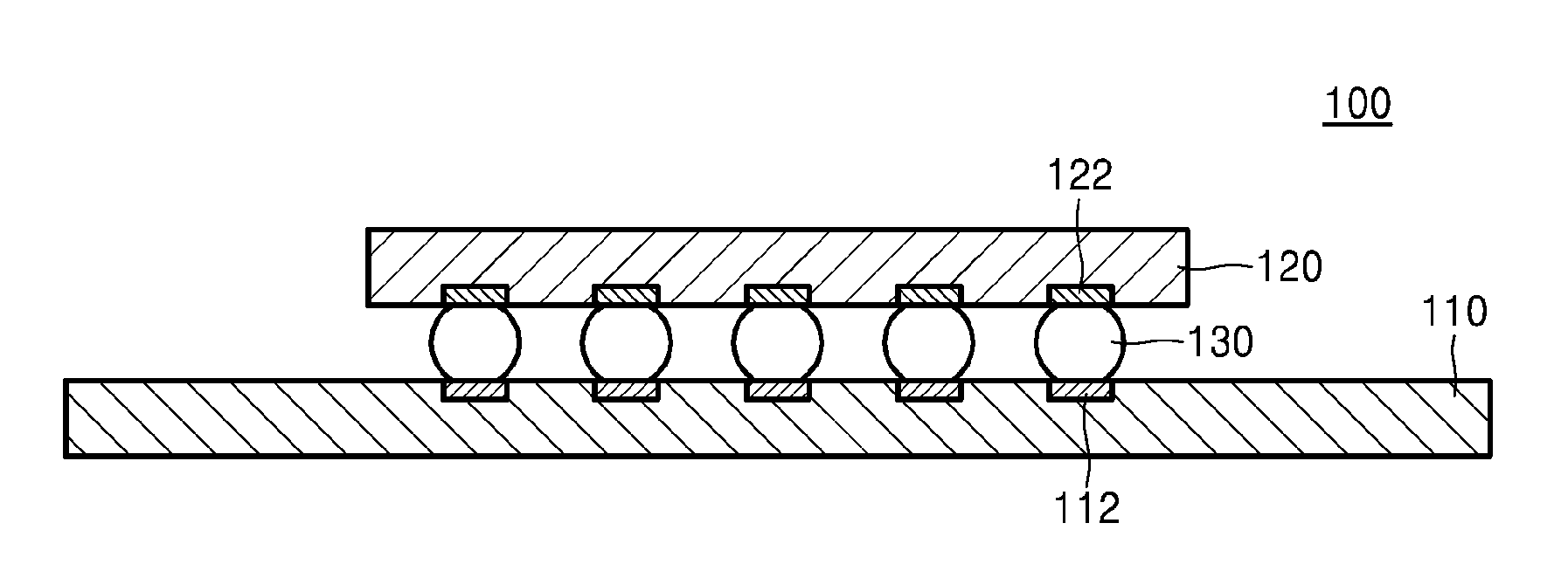
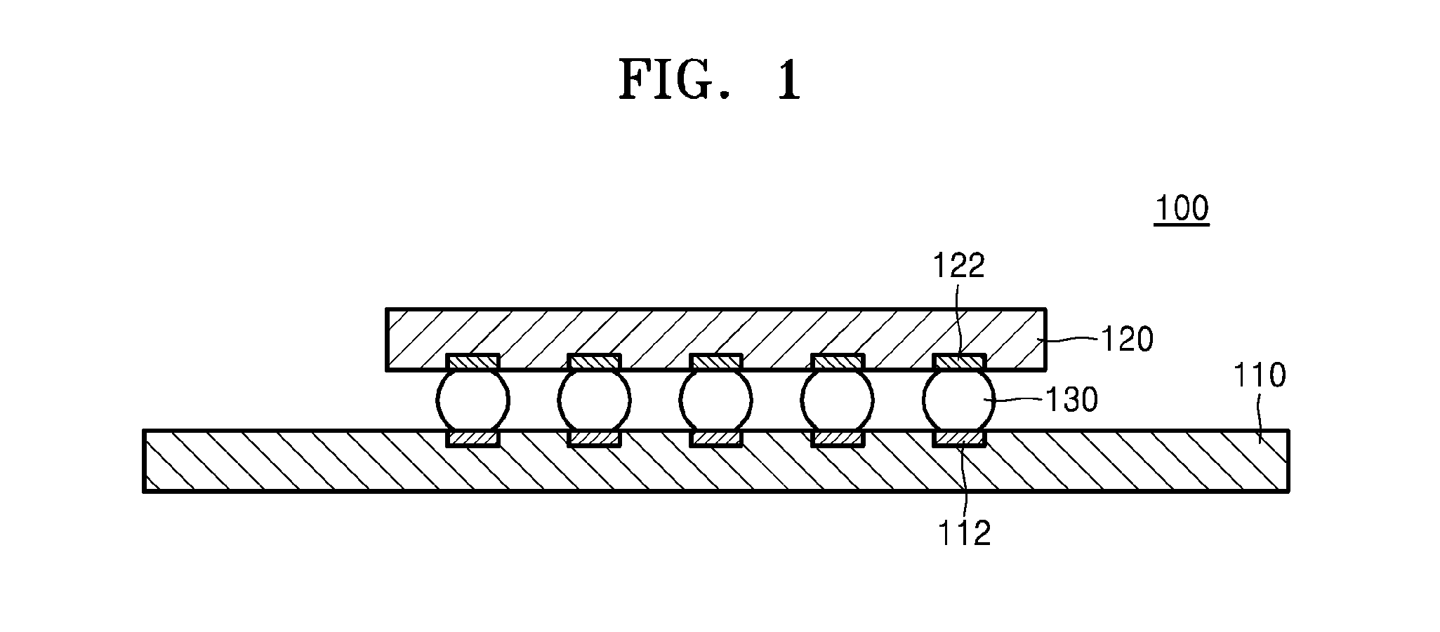
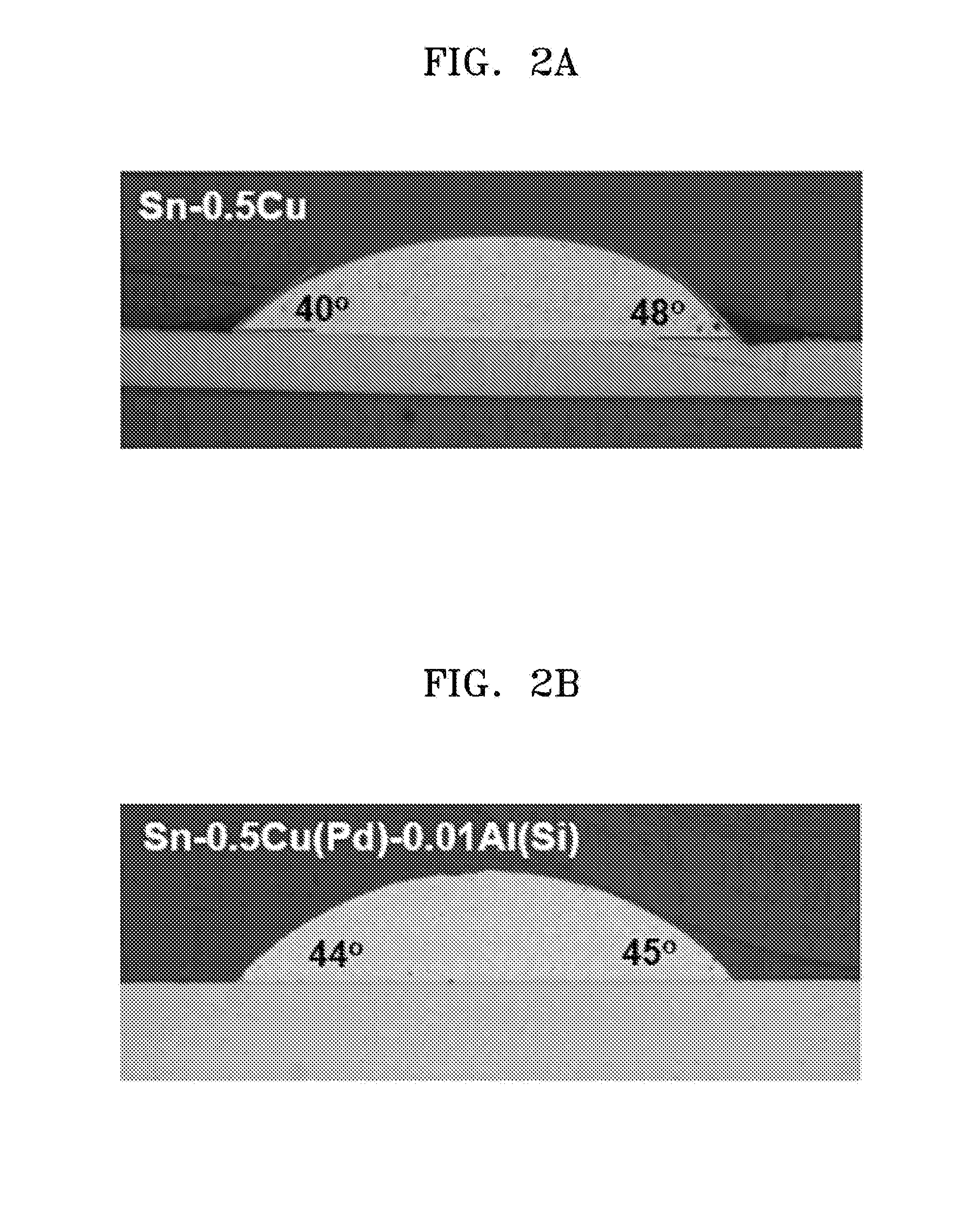
[0020]Reference will now be made in detail to embodiments, examples of which are illustrated in the accompanying drawings. In this regard, the present embodiments may have different forms and should not be construed as being limited to the descriptions set forth herein. These embodiments are provided so that this disclosure will be thorough and complete, and will fully convey the scope of the invention to one of ordinary skill in the art. Like reference numerals refer to like elements throughout. In the drawings, various elements and regions are schematically drawn. Accordingly, the embodiments according to the inventive concept are not limited to the relative sizes and gaps depicted in the accompanying drawings.

[0021]It will be understood that, although the terms ‘first’, ‘second’, etc. may be used herein to describe various elements, these elements should not be limited by these terms. These terms are only used to distinguish one element from another. For example, a first element ...


PUM

PropertyMeasurementUnit
Percent by massaaaaaaaaaa
Elongationaaaaaaaaaa

Abstract

Provided are a lead-free solder, a solder paste, and a semiconductor device, and more particularly, a lead-free solder that includes Cu in a range from about 0.1 wt % to about 0.8 wt %, Pd in a range from about 0.001 wt % to about 0.1 wt %, Al in a range from about 0.001 wt % to about 0.1 wt %, Si in a range from about 0.001 wt % to about 0.1 wt %, and Sn and inevitable impurities as remainder, a solder paste and a semiconductor device including the lead-free solder. The lead-free solder and the solder paste are environment-friendly and have a high high-temperature stability and high reliability.

Description

RELATED APPLICATION[0001]This application claims the benefit of Korean Patent Application No. 10-2013-0149999, filed on Dec. 4, 2013, in the Korean Intellectual Property Office, the disclosure of which is incorporated herein in its entirety by reference.BACKGROUND[0002]1. Field[0003]One or more exemplary embodiments relate to a lead-free solder, a solder paste, and a semiconductor device.[0004]2. Description of the Related Art[0005]Printed circuit boards (PCBs) have been widely used in home appliances, such as televisions, mobile phones, or computers. Recently, a lot of PCBs have been used in automobiles. For solders that are used in home appliances, a lot of Sn—Pb alloy group products have been used. In particular, lead (Pb) acts as a component that determines wettability, strength, and mechanical characteristics of a Sn—Pb alloy. Also, since lead is included in the Sn—Pb alloy, the melting point of the solder may be lowered to 183° C., and thus, thermal damage that occurs in a sol...

Claims


Application Information

Patent Timeline
IPC IPC(8): B23K35/26H01L23/00B23K35/02
CPCB23K35/262B23K35/025H01L24/17B23K2201/40H01L2924/01046H01L2924/01013H01L2224/16227H01L2924/0105H01L2924/01032H01L2924/01083H01L2924/01015H01L2924/014H01L2224/13147H01L2924/01014B23K35/362B23K2101/42B23K1/0016B23K2101/40C22C13/00H01L24/13H01L24/16H01L2224/13111H01L2224/16225H01L2224/81191H01L2224/81815H01L2924/15747H01L2924/00H01L2924/01029
Inventor HONG, SUNG JAEKIM, KEUN SOOLEE, CHANG WOOBANG, JUNG HWANKO, YONG HOLEE, HYUCK MOCHANG, JAE WONKOO, JA HYUNMOON, JEONG TAKLEE, YOUNG WOOHONG, WON SIKKIM, HUI JOONGLEE, JAE HONG
Owner MK ELECTRON
Why Eureka
Try Eureka