Defect classifying method and inspection apparatus

a technology of inspection apparatus and classification method, which is applied in the direction of optical radiation measurement, instruments, spectrometry/spectrophotometry/monochromators, etc., can solve the problem that the inspection apparatus cannot clearly detect the dislocation of the basal plane, the device characteristics change, and the performance of the element performance. problem, to achieve the effect of improving the classification accuracy

Active Publication Date: 2015-06-18
LASERTEC CORP
View PDF6 Cites 28 Cited by
  • Summary
  • Abstract
  • Description
  • Claims
  • Application Information

AI Technical Summary

Benefits of technology

[0025]Since the defect image of the reflection image and the defect image of the photoluminescence image are individually formed, it is necessary to provide a unit that associates the defect images with each other. Accordingly, in the present invention, the defect image of the reflection image and the defect image of the photoluminescence image are associated with each other by using the address information indicating the position of each defect image. Further, information including the address of each defect is used as the defect information to be classified. This configuration makes it possible to classify the defect based on the presence or absence of a defect image at a defect site, which is designated by the address information indicating the position of the defect, and based on the shape of the defect image.
[0026]According to the present invention, a change in minute unevenness of the surface of the epitaxial layer formed on the silicon carbide substrate is detected in the reflection image, and a change in the crystal structure within the epitaxial layer is detected in the photoluminescence image. This makes it possible to simultaneously detect both a defect appearing on the surface of the substrate and a defect existing only in the substrate. As a result, defects can be classified based on a lot of defect information, leading to a further improvement in the classification accuracy.

Problems solved by technology

Especially, in the case of producing a bipolar high-voltage element, a basal plane dislocation (BPD) is a killer defect which has an adverse effect on the performance of the element.
Specifically, in the case where a bipolar device is formed in an area including the BPD, when a current flows in the forward direction, the BPD is changed to a Shockley-type stacking fault, which causes a change in device characteristics and leads to a malfunction.
Accordingly, the inspection apparatus that uses the differential interference optical system has a drawback that the inspection apparatus cannot clearly detect the basal plane dislocations.
However, a carrot defect also exists as a crystal defect specific to the epitaxial layer formed on the SiC substrate.
A carrot defect is also a killer defect in the device production process, and thus the carrot defect needs to be detected in the defect inspection process.
However, the cause of occurrence of the carrot defect and the measures to prevent the occurrence of the carrot defect are different from those of the BPD.
However, since both the PL image of the BPD and the carrot defect are line-shaped images, it is actually difficult to detect the BPD and the carrot defect by distinguishing them from each other in the photoluminescence light inspection.

Method used


Image

  • Defect classifying method and inspection apparatus
  • Defect classifying method and inspection apparatus
  • Defect classifying method and inspection apparatus

Examples


first modified example

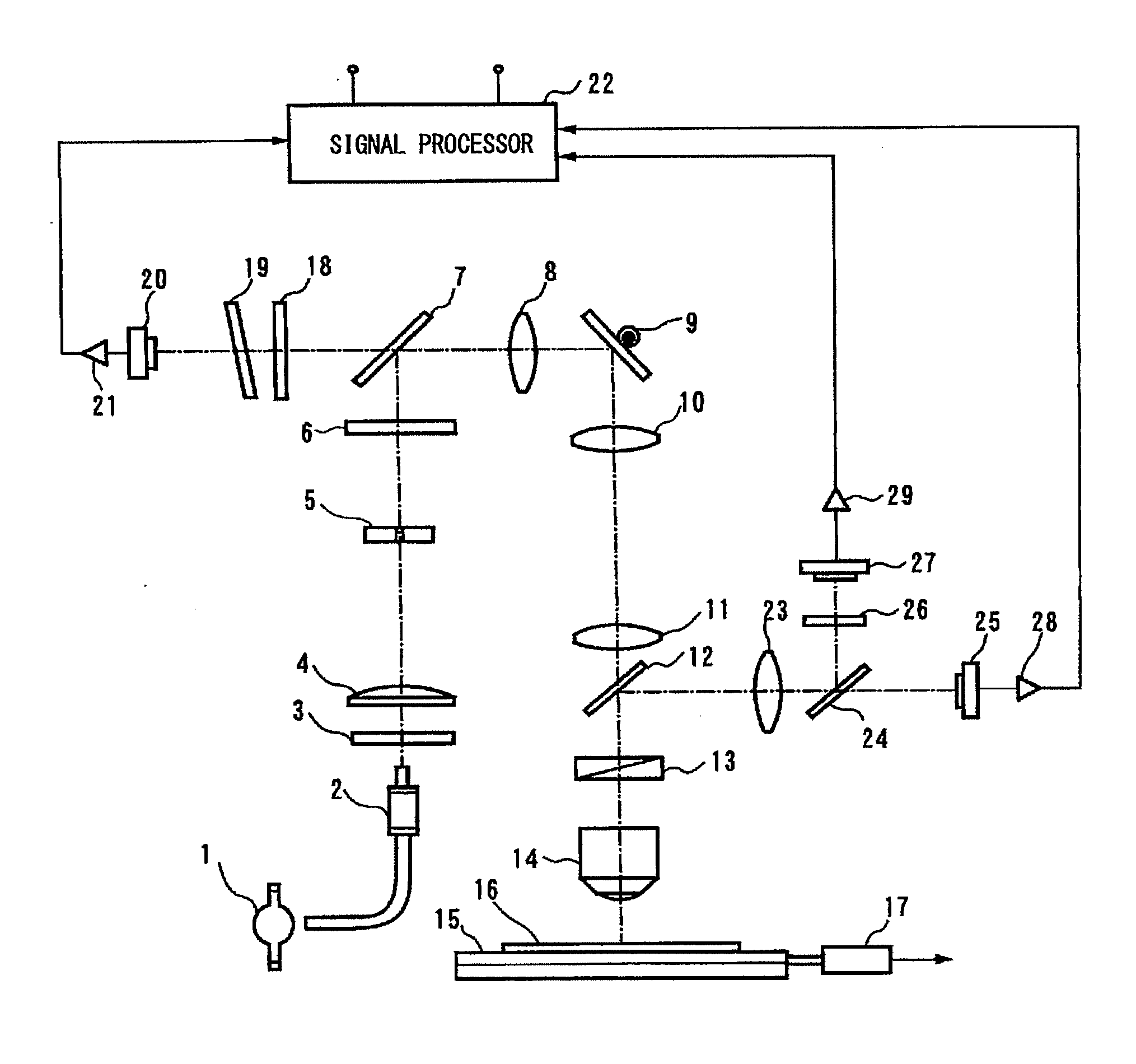
[0075]FIG. 5 is a diagram showing a first modified example of the inspection apparatus according to the present invention. The components of the first modified example identical to those shown in FIG. 1 are denoted by the same reference numerals, and the description thereof is omitted. In this example, a first illumination system that forms a reflection image and a second illumination system that forms a photoluminescence image are used. In the first illumination system, the surface of the substrate is scanned with the illumination beam of the visible region. In the second illumination system, the surface of the substrate is scanned with the illumination beam of the ultraviolet region. The first and second illumination beams are illuminated at the same location on the silicon carbide substrate 16.

[0076]The reflected light inspection is performed by using a mercury lamp 50 as the illumination light source and by using the visible light having a wavelength of 546 nm and emitted from t...

second modified example

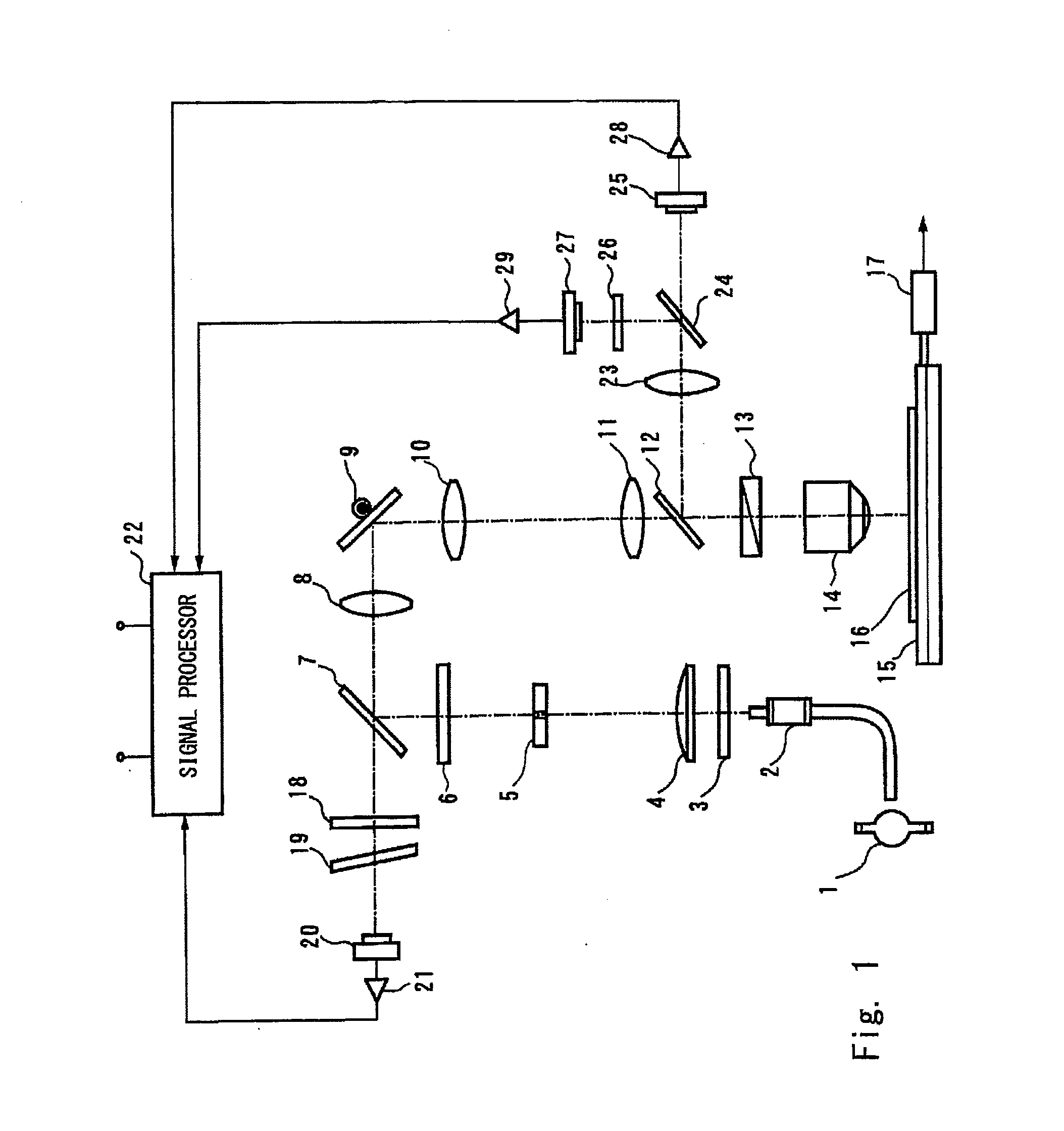
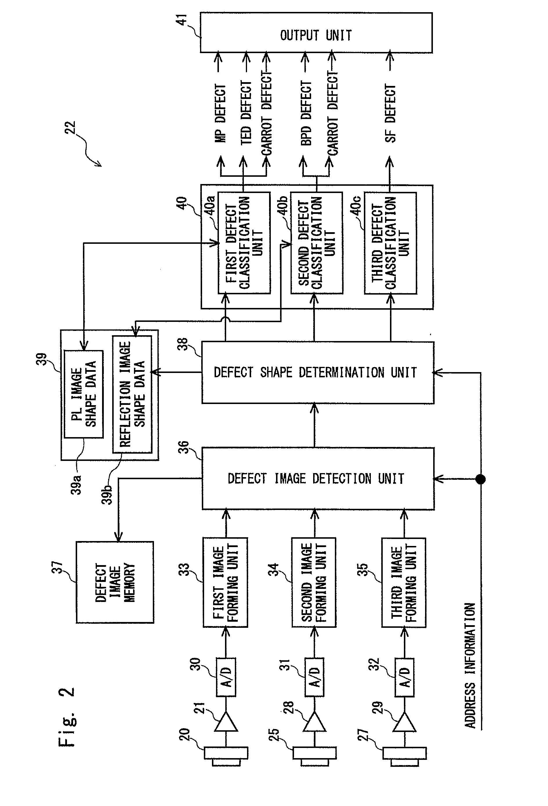
[0083]FIG. 6 shows a second modified example of the inspection apparatus according to the present invention. In this example, an illumination beam is obliquely projected on the surface of the silicon carbide substrate 16. A reflection image, a scattered light image, and a photoluminescence image are individually captured. The inspection apparatus detects defect images from these images. The inspection apparatus classifies each defect based on the defect image of the photoluminescence image and the defect image of the reflection image. Further, the inspection apparatus classifies each defect based on the defect image of the photoluminescence image and the defect image of the scattered light image. These images are associated with each other by using address information on each of the detected defect images.

[0084]A laser light source 70 that emits illumination light of the ultraviolet region is used as the illumination light source. The illumination beam emitted from the laser light s...

third modified example

[0088]FIG. 7 shows a third modified example of the inspection apparatus according to the present invention. In this example, an objective mirror is used instead of the objective lens. Scattered light and photoluminescence light, which are emitted from the silicon carbide substrate 74, are detected through the objective mirror. Defects are detected using a scattered light image and a photoluminescence image, and the detected defects are classified. The components of the third modified example identical to those shown in FIG. 6 are denoted by the same reference numerals, and the description thereof is omitted. A laser light source 90 that emits illumination light of the ultraviolet region is used as the illumination light source. The illumination beam emitted from the laser light source 90 passes through a polarizer 91 and is converted into a convergent beam by a lens 92. The illumination beam emitted from the lens 92 is obliquely projected toward the silicon carbide substrate 74. The...


PUM

PropertyMeasurementUnit
wavelengthaaaaaaaaaa
band-edge emission wavelengthaaaaaaaaaa

Abstract

Provided are a defect classifying method and an inspection apparatus which are capable of classifying a defect by distinguishing a basal plane dislocation, which is a killer defect in bipolar high-voltage elements, from other defects. The defect classifying method according to the present invention includes: projecting an illumination beam toward a silicon carbide substrate and forming a reflection image and a photoluminescence image; a first inspection step of detecting a defect image from the reflection image formed; a second inspection step of detecting a defect image from the photoluminescence image formed; and a defect classification step of classifying detected defects based on whether or not the defect image is detected and the shape of the detected defect image.

Description

INCORPORATION BY REFERENCE[0001]This application is based upon and claims the benefit of priority from Japanese patent application No. 2013-261652, filed on Dec. 18, 2013, and Japanese patent application No. 2014-199771, filed on Sep. 30, 2014, the disclosure of which is incorporated herein in its entirety by reference.BACKGROUND OF THE INVENTION[0002]1. Field of the Invention[0003]The present invention relates to a defect classifying method and an inspection apparatus that detect a defect which is present at a silicon carbide substrate (SiC substrate) and classify the detected defect.[0004]2. Description of Related Art[0005]Silicon carbide has superior physical and thermal properties, and thus is useful for production of a high-voltage, low-loss semiconductor device. In a semiconductor device production process using a SiC substrate, detection of defects which are present at the SiC substrate and classification of the defects which are detected are extremely important with regard t...

Claims


Application Information

Patent Timeline
Patent Type & Authority Applications(United States)
IPC IPC(8): G01N21/95G01N21/88
CPCG01N21/9501G01N21/8851G01N2201/12G01N2201/10G01N2201/06113G01N21/6489
Inventor SEKI, HIROKAZUSHINODA, MASAMICHITODOROKI, TOSHIYUKINAKANO, YOSHIHIROTORIZAWA, MAKOTO
Owner LASERTEC CORP
Why Eureka
Try Eureka