Optical imaging lens and electronic device comprising the same

Active Publication Date: 2015-07-02
GENIUS ELECTRONICS OPTICAL CO LTD
View PDF9 Cites 7 Cited by
  • Summary
  • Abstract
  • Description
  • Claims
  • Application Information

AI Technical Summary

Benefits of technology

[0008]In light of the above, the present invention proposes an optical imaging lens set that is lightweight, has shorter total length, has a low production cost, has an enlarged half of field of view, has a high resolution and has high image quality. The o

Problems solved by technology

The size of the optical imaging lens set is too big to satisfy

Method used


Image

  • Optical imaging lens and electronic device comprising the same
  • Optical imaging lens and electronic device comprising the same
  • Optical imaging lens and electronic device comprising the same

Examples


Example

First Example

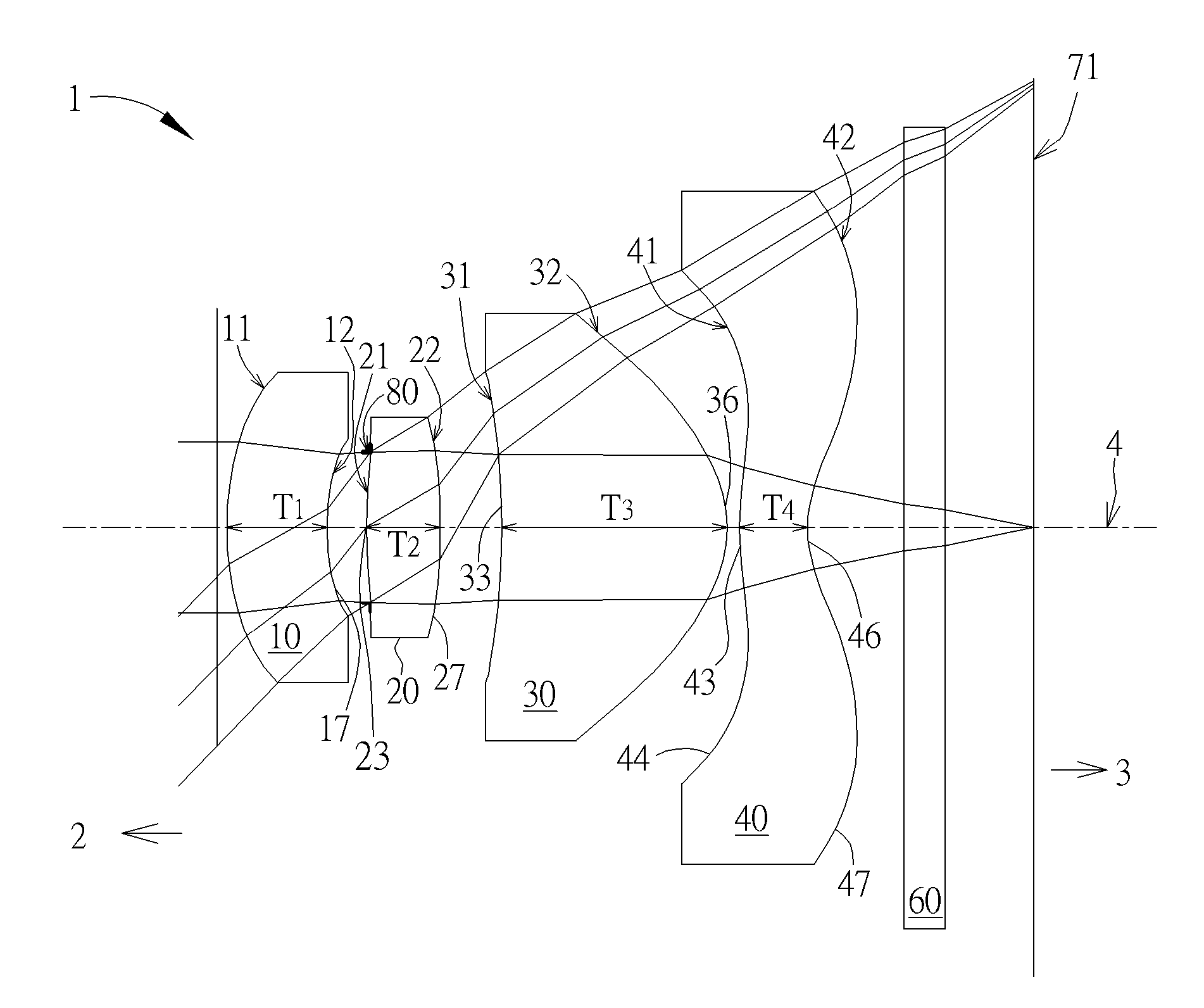
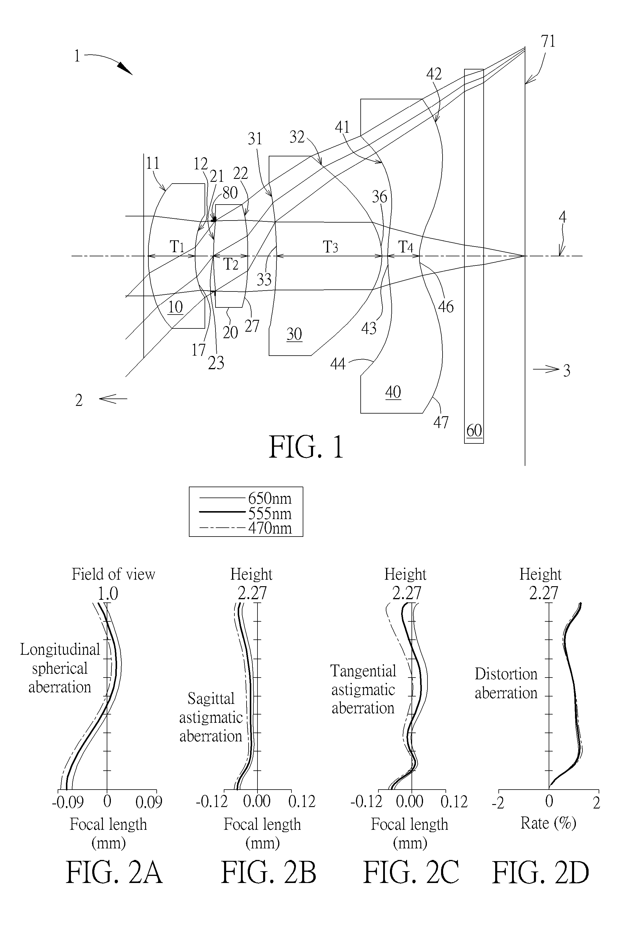
[0089]Please refer to FIG. 1 which illustrates the first example of the optical imaging lens set 1 of the present invention. Please refer to FIG. 2A for the longitudinal spherical aberration on the image plane 71 of the first example; please refer to FIG. 2B for the astigmatic field aberration on the sagittal direction; please refer to FIG. 2C for the astigmatic field aberration on the tangential direction, and please refer to FIG. 2D for the distortion aberration. The Y axis of the spherical aberration in each example is “field of view” for 1.0. The Y axis of the astigmatic field and the distortion in each example stand for “image height”.

[0090]The optical imaging lens set 1 of the first example has four lens elements 10 to 40, and all of the lens elements are made of a plastic material and have refractive power. The optical imaging lens set 1 also has an aperture stop 80, a filter 60, and an image plane 71. The aperture stop 80 is provided between the first lens eleme...

Example

Second Example

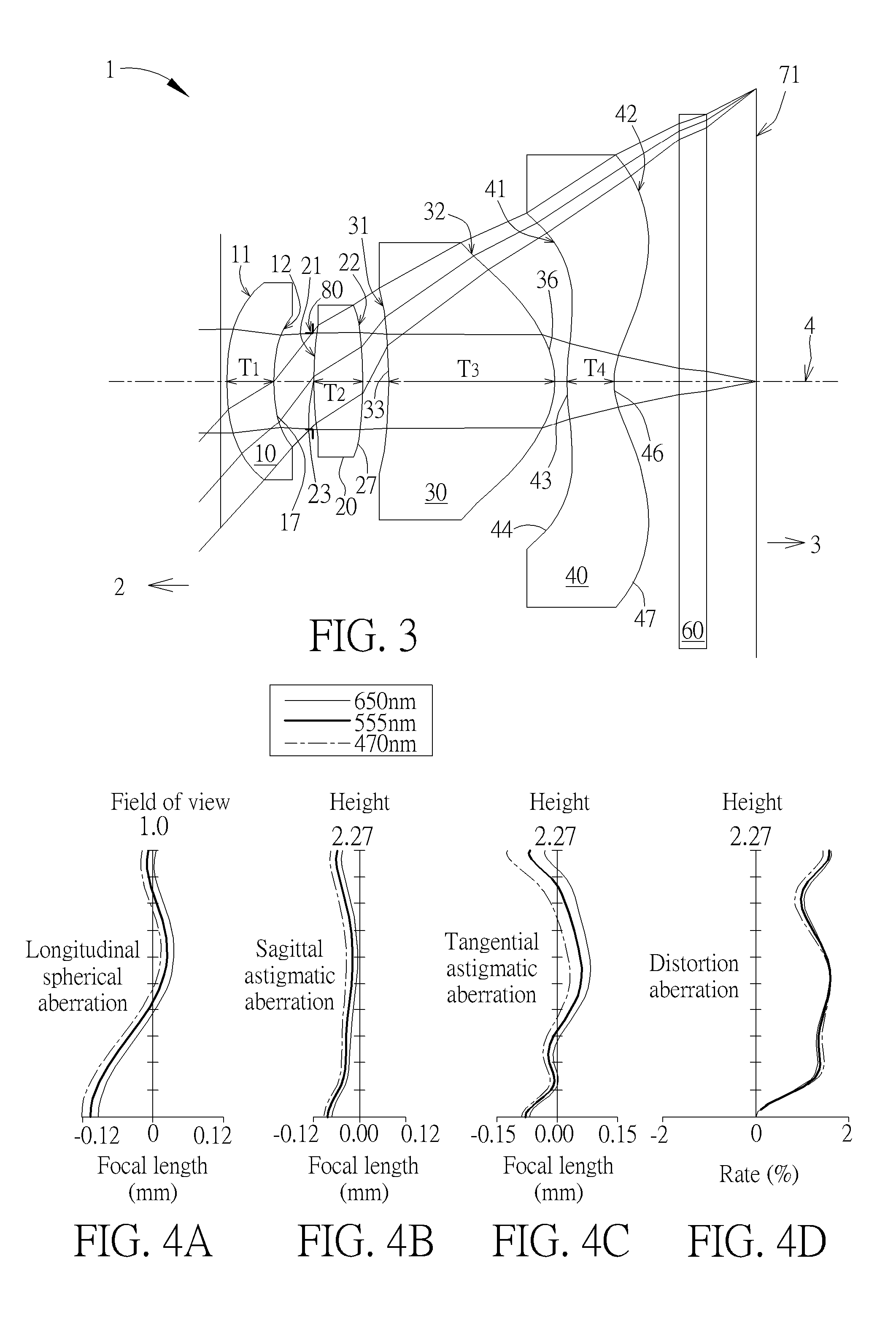
[0103]Please refer to FIG. 3 which illustrates the second example of the optical imaging lens set 1 of the present invention. Please refer to FIG. 4A for the longitudinal spherical aberration on the image plane 71 of the second example; please refer to FIG. 4B for the astigmatic aberration on the sagittal direction; please refer to FIG. 4C for the astigmatic aberration on the tangential direction, and please refer to FIG. 4D for the distortion aberration. The components in the second example are similar to those in the first example, but the optical data such as the curvature radius, the refractive power, the lens thickness, the lens focal length, the aspheric surface or the back focal length in this example are different from the optical data in the first example. The optical data of the second example of the optical imaging lens set are shown in FIG. 20 while the aspheric surface data are shown in FIG. 21. The length of the optical imaging lens set is 4.112 mm. The i...

Example

Third Example

[0104]Please refer to FIG. 5 which illustrates the third example of the optical imaging lens set 1 of the present invention. Please refer to FIG. 6A for the longitudinal spherical aberration on the image plane 71 of the third example; please refer to FIG. 6B for the astigmatic aberration on the sagittal direction; please refer to FIG. 6C for the astigmatic aberration on the tangential direction, and please refer to FIG. 6D for the distortion aberration. The components in the third example are similar to those in the first example, but the optical data such as the curvature radius, the refractive power, the lens thickness, the lens focal length, the aspheric surface or the back focal length in this example are different from the optical data in the first example. The optical data of the third example of the optical imaging lens set are shown in FIG. 23 while the aspheric surface data are shown in FIG. 24. The length of the optical imaging lens set is 3.811 mm. The image ...


PUM


Abstract

An optical imaging lens set includes a first lens element with a concave image-side surface in a vicinity of its periphery, a second lens element with a convex object-side surface in a vicinity of the optical axis and a convex image-side surface in a vicinity of its periphery, a third lens element with positive refractive power, a concave object-side surface in a vicinity of the optical axis and a convex image-side surface in a vicinity of the optical axis and a fourth lens element with a concave image-side surface in a vicinity of the optical axis and a convex image-side surface in a vicinity of its periphery.

Description

CROSS REFERENCE TO RELATED APPLICATION[0001]This application claims priority to Chinese Application No. 201310746543.3, filed on Dec. 30, 2013.BACKGROUND OF THE INVENTION[0002]1. Field of the Invention[0003]The present invention generally relates to an optical imaging lens set and an electronic device which includes such optical imaging lens set. Specifically speaking, the present invention is directed to an optical imaging lens set with shorter length and an electronic device which includes such optical imaging lens set.[0004]2. Description of the Prior Art[0005]In recent years, the popularity of mobile phones and digital cameras makes photography modules (including optical imaging lens set, holder and sensor, etc) well developed. Mobile phones and digital cameras become lighter and thinner, so the miniaturization demands of photography modules get higher and higher. As the charge coupled device (CCD) or complementary metal-oxide semiconductor (CMOS) technologies advance, the size ...

Claims


Application Information

Patent Timeline
IPC IPC(8): G02B13/00G02B7/02G03B30/00
CPCG02B13/004G02B9/58G02B9/34
Inventor WANG, KAI LUNYE, LONGCHEN, YANBIN
Owner GENIUS ELECTRONICS OPTICAL CO LTD
Why Eureka
Try Eureka