Organic photoelectronic device and image sensor
a photoelectronic device and image sensor technology, applied in thermoelectric devices, solid-state devices, radiation control devices, etc., can solve problems such as deterioration of sensitivity, achieve the effects of reducing leakage current, ensuring photoelectric conversion efficiency, and reducing incident light loss
- Summary
- Abstract
- Description
- Claims
- Application Information
AI Technical Summary
Benefits of technology
Problems solved by technology
Method used
Image
Examples
example 1
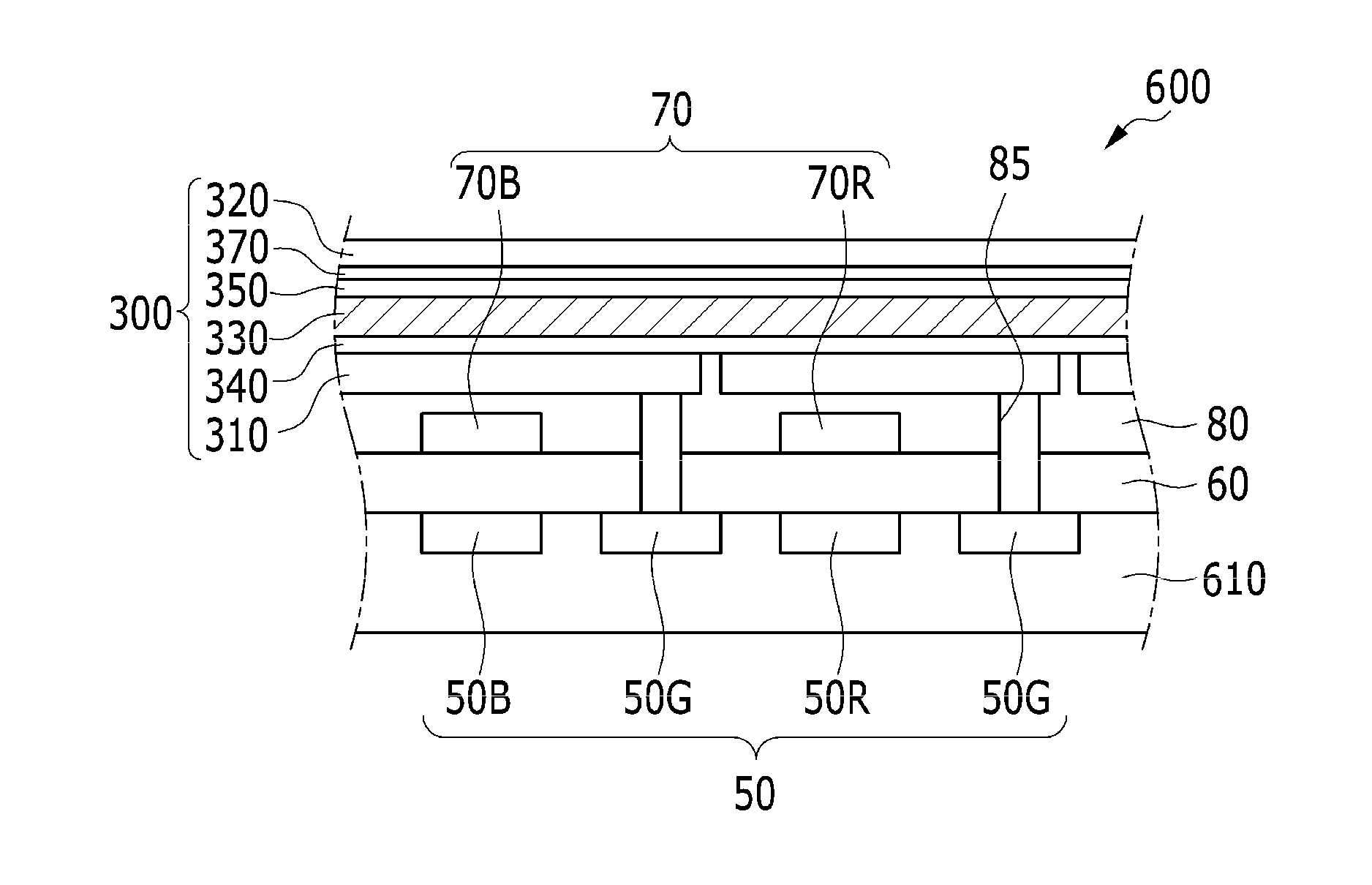
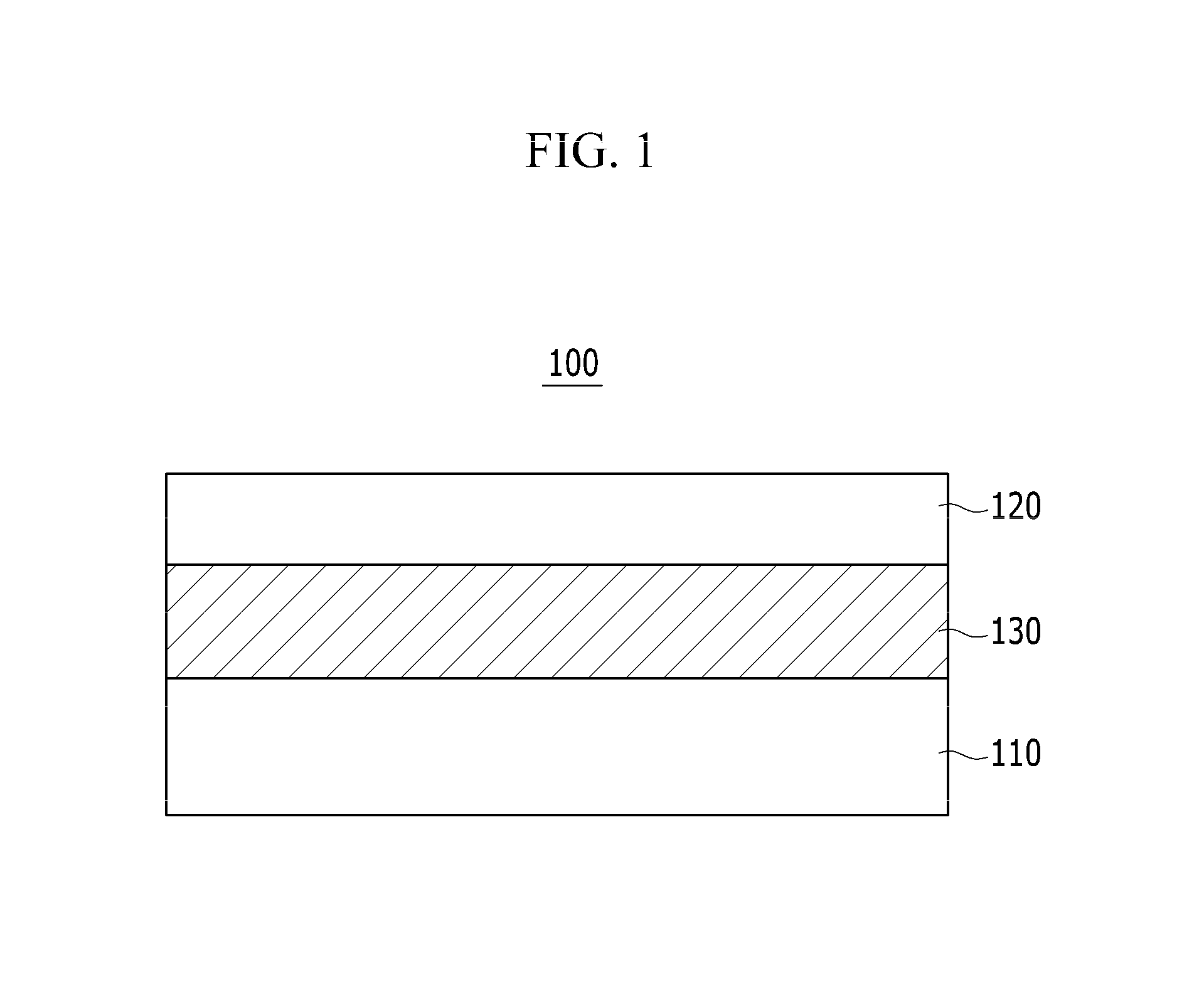
[0124]A lower electrode that is about 100 nm-thick is formed by sputtering ITO on a glass substrate. Subsequently, a 5 nm-thick lower charge auxiliary layer is formed on the lower electrode by thermally evaporating molybdenum oxide (MoOx, 02: 0.2 sccm), manufacturing an organic photoelectronic device.
example 2
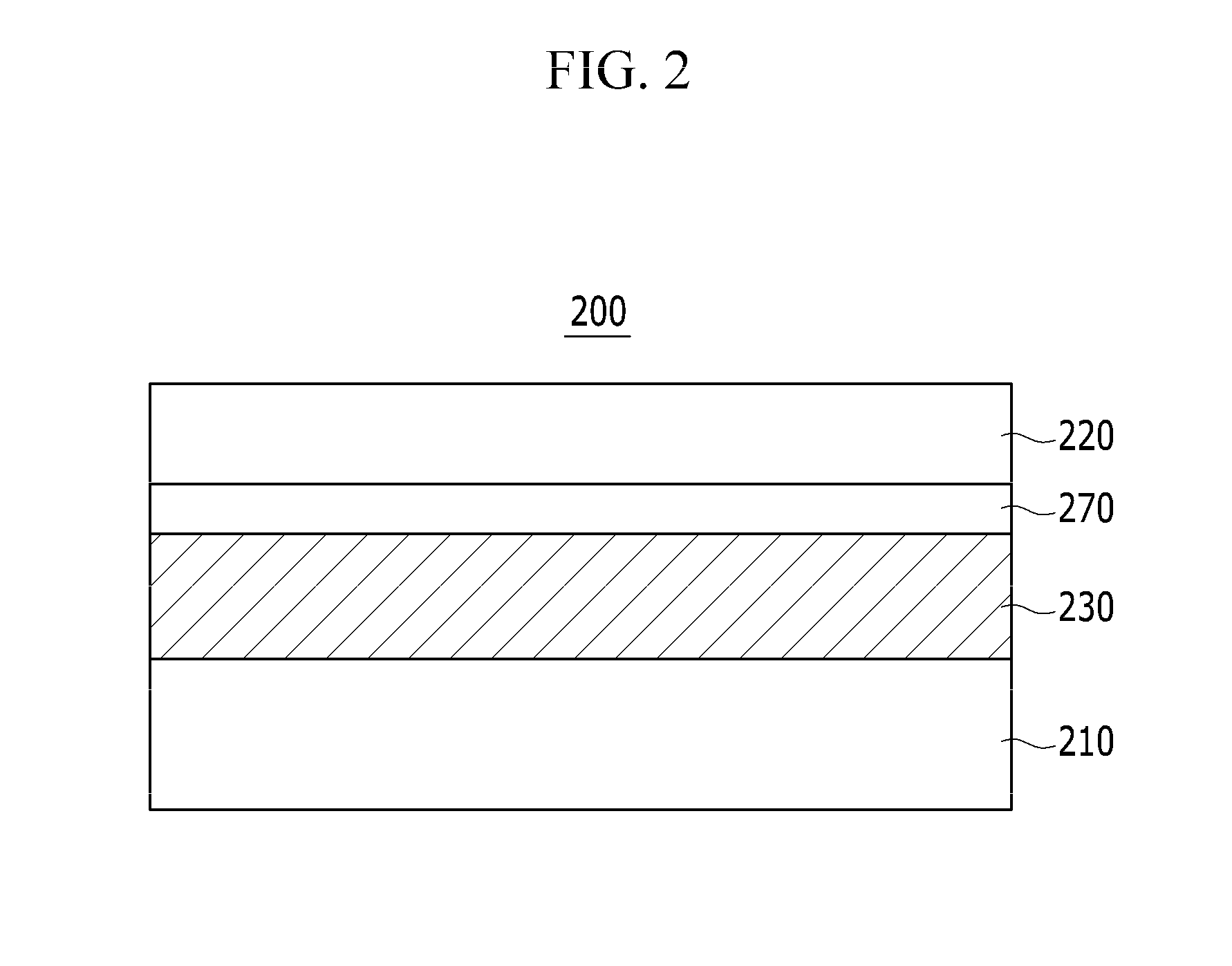
[0125]An organic photoelectronic device is manufactured according to the same example method as in Example 1, except for additionally forming a buffer layer by thermally evaporating molybdenum oxide (MoOx, 0<x≦3) to be about 10 nm thick before forming the upper electrode.
example 3
[0126]An organic photoelectronic device is manufactured according to the same example method as Example 1, except for additionally forming a buffer layer by thermally evaporating tungsten oxide (WOx, 0<x≦3) to be about 10 nm thick before forming the upper electrode.
PUM
 Abstract
Description
Claims
Application Information


