Integral fabrication of asymmetric CMOS transistors for autonomous wireless state radios and sensor/actuator nodes

a technology of cmos transistor and autonomous wireless state radio, applied in the field of logic circuits, can solve the problems of higher average power consumption, dominance of static power consumption, and dominance of average power consumption in the fig. 1 of circuits fabricated using advanced cmos technology

Inactive Publication Date: 2015-07-30
QUALCOMM TECH INT
View PDF5 Cites 59 Cited by
  • Summary
  • Abstract
  • Description
  • Claims
  • Application Information

AI Technical Summary

Problems solved by technology

Typically static power consumption dominates over the active switching power in this case.
Due to higher static power consumption, the average power consumption can be dominated by the leakage power consumed by circuits that remain powered during the sleep.
This is seen by the higher average power consumption in FIG. 1 for circuits fabricated using advanced CMOS technology compared to those fabricated using conventional CMOS technology.
However, the resulting highly doped, abrupt junctions cause significant junction leakage.

Method used


Image

  • Integral fabrication of asymmetric CMOS transistors for autonomous wireless state radios and sensor/actuator nodes
  • Integral fabrication of asymmetric CMOS transistors for autonomous wireless state radios and sensor/actuator nodes
  • Integral fabrication of asymmetric CMOS transistors for autonomous wireless state radios and sensor/actuator nodes

Examples


Embodiment Construction

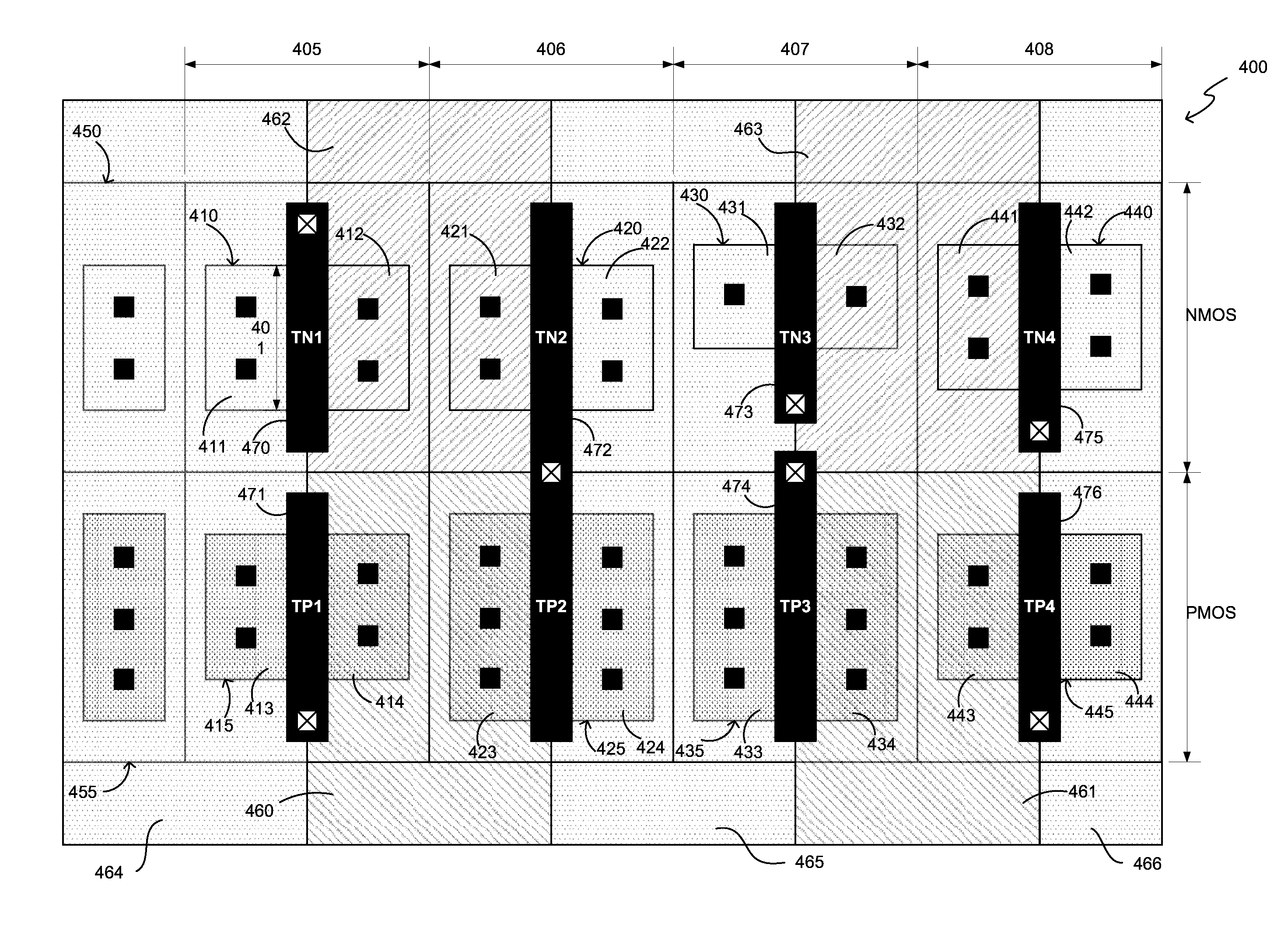
[0029]FIG. 3A shows a thin gate-oxide transistor 10 in which the source region 20 is fabricated with a pocket implant 25. The drain region 30 of the transistor 10 is similarly fabricated with a pocket implant 35. Conventionally, the source and drain regions are implanted with the same masking step, and the implantation results in an extension of either region (see regions 25 and 35 in FIG. 3A). The resulting pocket implant and extension are coupled together for each of the source and drain regions. With reference to FIG. 3A, an embodiment of the present invention is shown in FIG. 3B in which the doping of the extension and pocket implant 25 in the source region 20 is different to that of the extension and pocket implant 36 of the drain region (as indicated by the different shading for regions 35 and 36 in FIGS. 3A and 3B).

[0030]Standard CMOS fabrication technologies use multiple pocket and extension implants to realise a desired threshold voltage VT. In the conventional transistor o...


PUM


Abstract

A method of arranging asymmetrically doped CMOS transistors in a semiconductor wafer that forms base cells within a plurality of logic standard cells in a CMOS process technology that includes conventional symmetric CMOS transistors having different threshold voltages. The asymmetrically doped CMOS transistors have a gate length exceeding 1.5 times the minimum gate length of the symmetric CMOS transistors. Regions defined by electrical junctions directly adjacent to the gate of the asymmetric transistors are formed by an implant mask exposing an area of the wafer on the source side of the transistor to receive the junction implant of the symmetric CMOS transistors with a higher threshold voltage while shielding the drain area, and a further implant mask exposing an area of the wafer on the drain side of the transistor to receive the junction implant of the symmetric CMOS transistors with a lower threshold voltage while shielding the source area.

Description

TECHNICAL FIELD[0001]The present disclosure relates to logic circuits constructed from asymmetrically doped complementary metal-oxide-semiconductor (CMOS) transistors. It is particularly related to, but in no way limited to, CMOS transistors used for autonomous wireless state radios and sensor actuator nodes.BACKGROUND[0002]Autonomous wireless state radios and sensor / actuator systems may be characterised by having no local user interfaces and are often required to be Always-ON. Always-ON in this context is characterised by long periods of standby (more than 99% of the time) with short bursts of activity, during which, for example, a transmission is made and / or measurements are taken or actuators operated.[0003]During standby, certain system functions have to be maintained. This critically involves, for example, scheduling of the next transmission and maintaining state information, but may also include continuous sensing.[0004]Advances in low power CMOS process technology have been d...

Claims


Application Information

Patent Timeline
Patent Type & Authority Applications(United States)
IPC IPC(8): G06F17/50
CPCG06F17/5072H01L2924/0002H01L21/823814H01L27/0207H01L29/1045G06F30/392H01L29/7835H01L27/092H01L2924/00H01L21/823418H01L29/66659H01L23/00
Inventor HERBERHOLZ, RAINER
Owner QUALCOMM TECH INT
Why Eureka
Try Eureka