Methods for etching a dielectric barrier layer in a dual damascene structure

a dielectric barrier layer and damascene technology, applied in the direction of electrical equipment, basic electric elements, electric discharge tubes, etc., can solve the problems of inoperable circuit, undesirable metal diffusion into the dielectric bulk insulating material, and degrade the overall performance of the integrated circui

Active Publication Date: 2015-07-30
APPLIED MATERIALS INC
View PDF2 Cites 60 Cited by
  • Summary
  • Abstract
  • Description
  • Claims
  • Application Information

AI Technical Summary

Benefits of technology

[0011]Methods for eliminating early exposure of a conductive layer in a dual damascene structure and for etching a dielectric barrier layer in the dual damascene structure are provided. In one embodiment, a method for etching a dielectric barrier layer disposed on a substrate includes patterning a substrate having a dielectric bulk insulating layer disposed on a dielectric barrier layer using a hardmask layer disposed on the dielectric bulk insulating layer as an etching mask, exposing a portion of the dielectric barrier layer after removing the dielectric bulk insulating layer uncovered by the dielectric bulk insulating layer, removing the hardmask layer from the substrate, and subsequently etching the dielectric barrier layer exposed by the dielectric bulk insulating layer.

Problems solved by technology

Reliably producing sub-half micron and smaller features is one of the key technology challenges for next generation very large scale integration (VLSI) and ultra large-scale integration (ULSI) of semiconductor devices.
However, as the limits of circuit technology are pushed, the shrinking dimensions of VLSI and ULSI interconnect technology have placed additional demands on processing capabilities.
Capacitive coupling between adjacent metal interconnects may cause cross talk and / or resistance-capacitance (RC) delay which degrades the overall performance of the integrated circuit and may render the circuit inoperable.
Diffusion of the metal into the dielectric bulk insulating material is undesirable because such diffusion can affect the electrical performance of the integrated circuit, or render the circuit inoperative.
However, early exposure of the underlying conductive layer may result in the conductive layer being subjected to oxidizing conditions during a subsequent etching process or excess exposure to the ambient environment, which may adversely accumulate native oxides or contaminants on the metal surface prior to a subsequent metallization process.
Excess native oxide accumulation or contaminants may adversely affect the nucleation capability of the metal elements to adhere to the substrate surface during the metallization process.
Furthermore, poor adhesion at the interface may also result in undesired high contact resistance, thereby resulting in undesirably poor electrical properties of the device.
In addition, poor nucleation of the metal elements in the back end interconnection may impact not only the electrical performance of the devices, but also on the integration of the conductive contact material subsequently formed thereon.

Method used


Image

  • Methods for etching a dielectric barrier layer in a dual damascene structure
  • Methods for etching a dielectric barrier layer in a dual damascene structure
  • Methods for etching a dielectric barrier layer in a dual damascene structure

Examples


Embodiment Construction

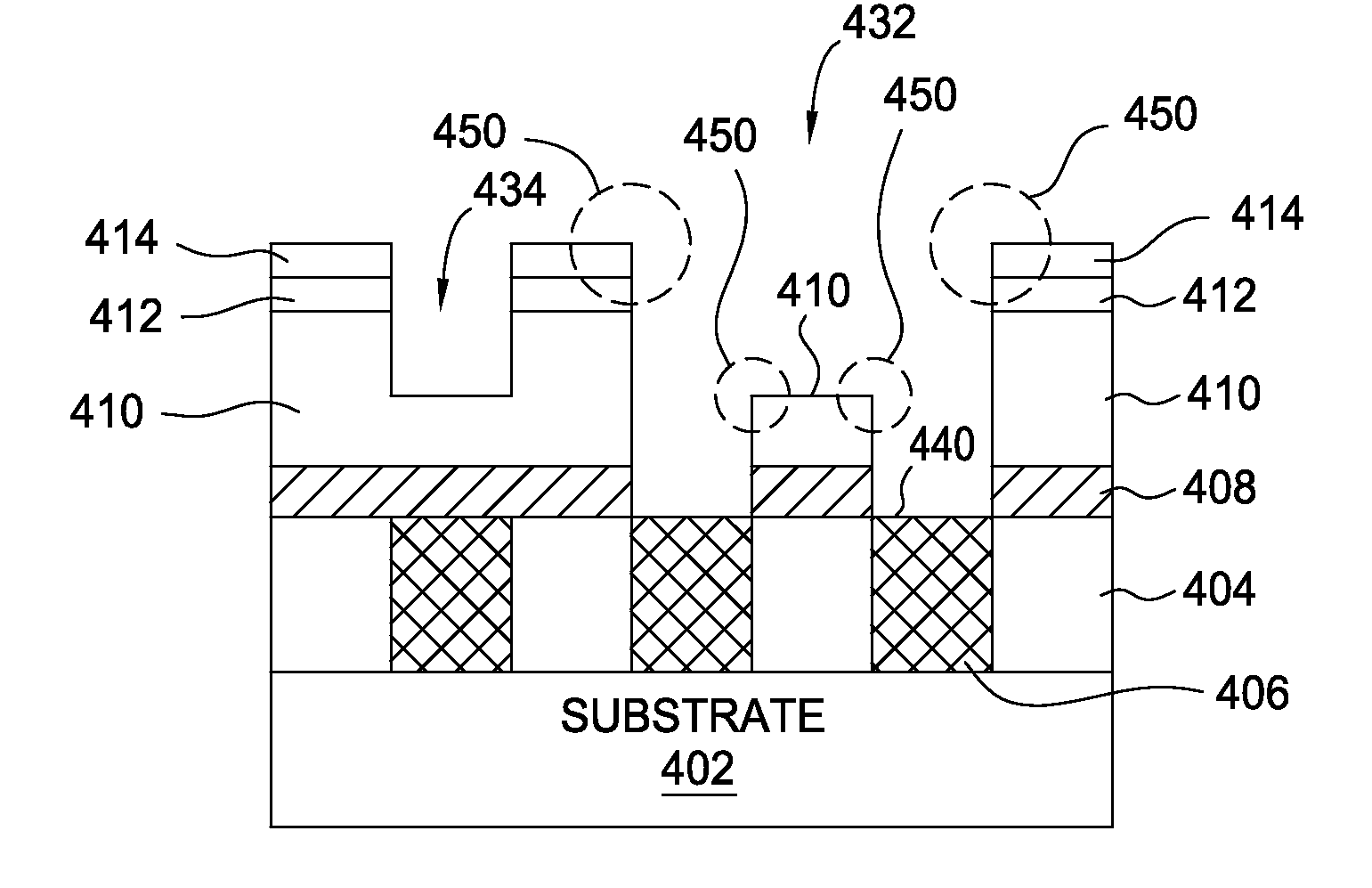
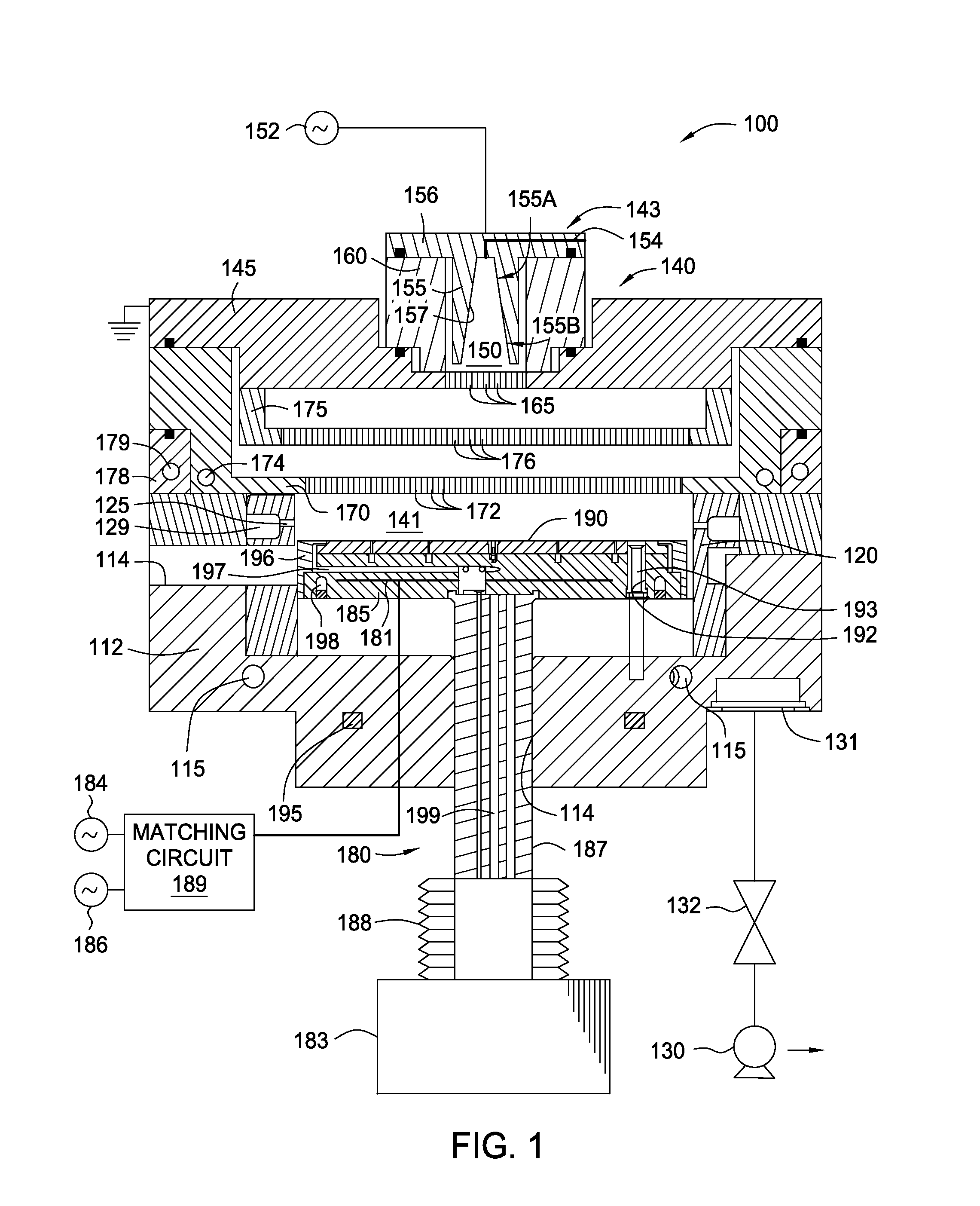
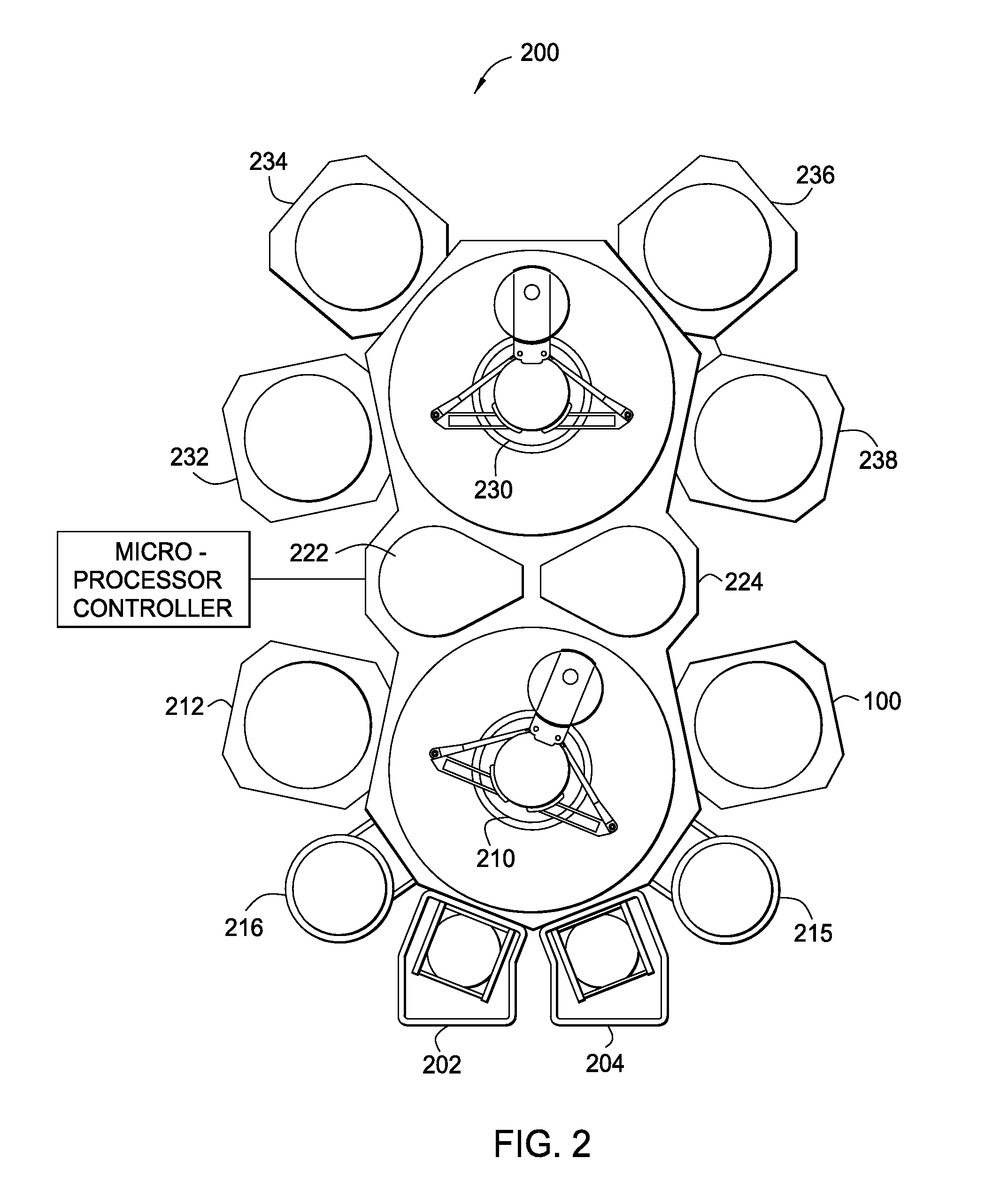
[0021]Methods for forming a dual damascene structure without early exposure to an underlying conductive layer formed in the dual damascene structure and for etching a dielectric barrier layer in the dual damascene structure are disclosed herein which provide an etching process with high etching selectivity and interface high quality after the dual damascene manufacturing process. In one embodiment, the dielectric barrier layer etching process includes a cyclic etching process to repetitively and incrementally etch the dielectric barrier layer until an underlying conductive layer is exposed. Furthermore, the sequence for etching film materials formed in the dual damascene structure is also arranged in a manner (known as “Barrier Open Last” process) to eliminate exposure time of the conductive layers after the dielectric barrier layer etching process. By utilizing an etching process with high etching selectivity along with the “Barrier Open Last” process sequence, a good interface con...


PUM


Abstract

Methods for eliminating early exposure of a conductive layer in a dual damascene structure and for etching a dielectric barrier layer in the dual damascene structure are provided. In one embodiment, a method for etching a dielectric barrier layer disposed on a substrate includes patterning a substrate having a dielectric bulk insulating layer disposed on a dielectric barrier layer using a hardmask layer disposed on the dielectric bulk insulating layer as an etching mask, exposing a portion of the dielectric barrier layer after removing the dielectric bulk insulating layer uncovered by the dielectric bulk insulating layer, removing the hardmask layer from the substrate, and subsequently etching the dielectric barrier layer exposed by the dielectric bulk insulating layer.

Description

CROSS-REFERENCE TO RELATED APPLICATIONS[0001]This application claims benefit of U.S. Provisional Application Ser. No. 61 / 931,445 filed Jan. 24, 2014 (Attorney Docket No. APPM / 21473L), which is incorporated by reference in their entirety.BACKGROUND OF THE INVENTION[0002]1. Field of the Invention[0003]Embodiments of the present invention generally relate to methods for forming semiconductor devices. More particularly, embodiments of the present invention generally relate to methods for etching a dielectric barrier layer without damaging underlying conductive structures for manufacturing semiconductor devices.[0004]2. Description of the Related Art[0005]Reliably producing sub-half micron and smaller features is one of the key technology challenges for next generation very large scale integration (VLSI) and ultra large-scale integration (ULSI) of semiconductor devices. However, as the limits of circuit technology are pushed, the shrinking dimensions of VLSI and ULSI interconnect technol...

Claims


Application Information

Patent Timeline
Patent Type & Authority Applications(United States)
IPC IPC(8): H01L21/768H01L21/02H01L21/033H01L21/311
CPCH01L21/3065H01L21/0234H01L21/308H01L21/76807H01L21/31138H01L21/31144H01L21/02063H01L21/0332H01L21/30604H01L21/31116H01J37/32357H01L21/76811H01L21/76813
Inventor REN, HEKAO, CHIA-LINGKANG, SEANPENDER, JEREMIAH T PNEMANI, SRINIVAS D.NAIK, MEHUL B.
Owner APPLIED MATERIALS INC
Why Eureka
Try Eureka