Finfet and method for manufacturing the same

Active Publication Date: 2015-08-06
INST OF MICROELECTRONICS CHINESE ACAD OF SCI
View PDF19 Cites 10 Cited by
  • Summary
  • Abstract
  • Description
  • Claims
  • Application Information

AI Technical Summary

Benefits of technology

This patent describes a new type of semiconductor device called a strained FinFET, which has improved performance. It includes a layer that applies stress to the device, which increases the mobility of electrical charges and reduces the resistance when the device is turned on. This results in faster switching speeds for the device.

Problems solved by technology

However, it is well known that short channel effects arise as the size of MOSFETs decreases.
However, it is difficult in the FinFET to apply the suitable stress to the channel region in a direction between a source region and a drain region.
In other words, the strained FinFET is still a challenge.

Method used


Image

  • Finfet and method for manufacturing the same
  • Finfet and method for manufacturing the same
  • Finfet and method for manufacturing the same

Examples


Embodiment Construction

[0019]Exemplary embodiments of the present disclosure will be described in more details below with reference to the accompanying drawings. In the drawings, like reference numerals denote like members. The figures are not drawn to scale for the sake of clarity.

[0020]For simplicity, the structure of the semiconductor device having been subject to several relevant processing steps may be shown in one figure.

[0021]It should be understood that when one layer or region is referred to as being “above” or “on” another layer or region in the description of a device structure, it can be directly above or on the other layer or region, or other layers or regions may be intervened therebetween. Moreover, if the device in the figures is turned over, the layer or region will be “under” or “below” the other layer or region.

[0022]In contrast, when one layer is referred to as being “directly on” or “on and adjacent to” or “adjoin” another layer or region, there are not intervening layers or regions p...


PUM


Abstract

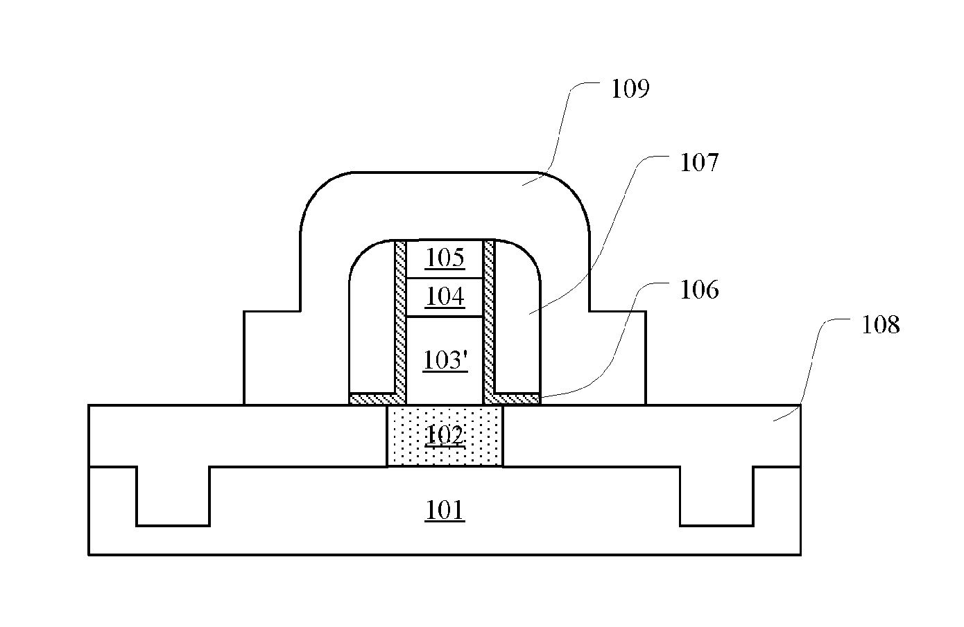
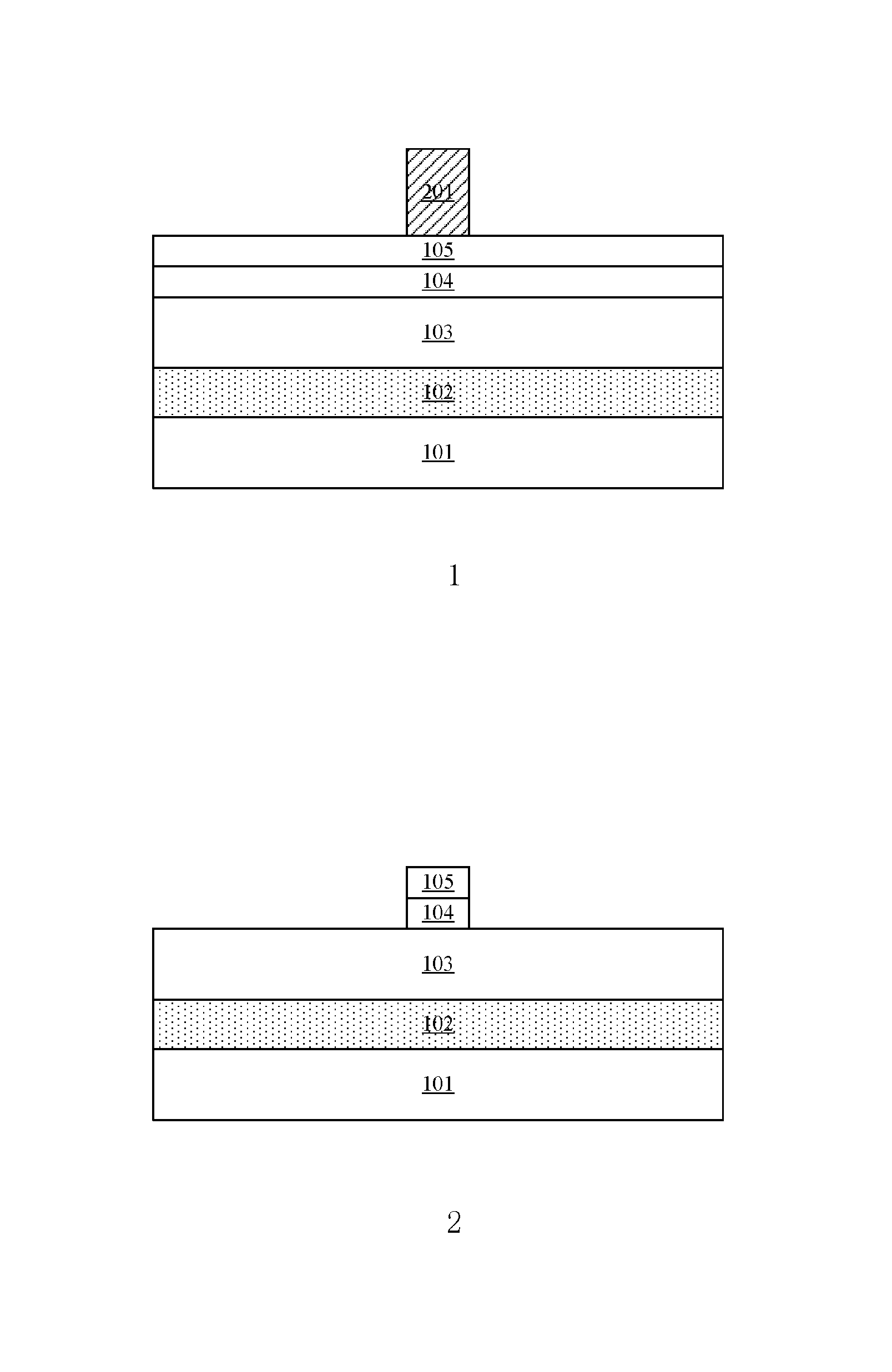
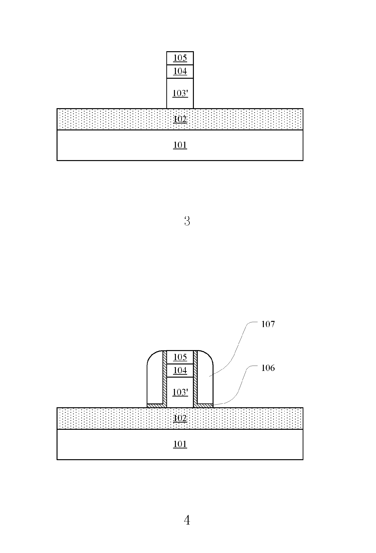
An FinFET and a method for manufacturing the same are disclosed. The FinFET comprises: a semiconductor substrate; a stress layer on the semiconductor substrate; a semiconductor fin on the stress layer, the semiconductor fin having two sidewalls extending in its length direction; a gate dielectric on the sidewalls of the semiconductor fin; a gate conductor on the gate dielectric; and a source region and a drain region at two ends of the semiconductor fin, wherein the stress layer extends below and in parallel with the semiconductor fin, and applies stress to the semiconductor fin in the length direction of the semiconductor fin.

Description

CROSS-REFERENCE TO RELATED APPLICATION(S)[0001]This application claims priority to the Chinese Patent Application No. 201210285604.6, filed on Aug. 10, 2012, entitled “FinFET AND METHOD FOR MANUFACTURING THE SAME”, which is incorporated herein by reference in its entirety.TECHNICAL FIELD[0002]The present disclosure relates to semiconductor technology, and in particular, to strained FinFETs and methods for manufacturing the same.BACKGROUND[0003]An important trend in development of semiconductor technology is scaling down of metal-oxide-semiconductor field effect transistors (MOSFETs) for improving integration level and reducing manufacturing cost. However, it is well known that short channel effects arise as the size of MOSFETs decreases. When the size of the MOSFET is scaled down, a gate of the MOSFET has a smaller effective length and actually controls fewer charges in a depletion region when a gate voltage is applied. Consequently, the MOSFET has a reduced threshold voltage with a...

Claims


Application Information

Patent Timeline
IPC IPC(8): H01L29/78H01L21/3065H01L29/06H01L21/308H01L29/66H01L29/161
CPCH01L29/785H01L29/1054H01L29/7846H01L29/66795H01L29/7849H01L29/0649H01L29/0611H01L21/308H01L21/3065H01L29/161H01L29/0603H01L29/7842H01L29/165
Inventor ZHU, HUILONGXU, MIAO
Owner INST OF MICROELECTRONICS CHINESE ACAD OF SCI
Why Eureka
Try Eureka