Temperature-Compensated Reference Voltage System With Very Low Power Consumption Based On An SCM Structure With Transistors Of Different Threshold Voltages

a reference voltage and very low power consumption technology, applied in the field of reference voltage circuits, can solve the problems of increasing power requirements of advanced systems, increasing power requirements, and tight levels, and evidencing a greater energy consumption required for systems to operate perfectly

Active Publication Date: 2015-08-20
CENT NACIONAL DE TECHA ELECTRONICSA AVANCADA
View PDF13 Cites 21 Cited by
  • Summary
  • Abstract
  • Description
  • Claims
  • Application Information

AI Technical Summary

Benefits of technology

[0016]In order to eliminate the inconvenience already known in the state of the art, this solution has the purpose of pro

Problems solved by technology

The power required by advanced systems has achieved increasingly low and tight levels, particularly in RF and biomedical system applications due to the limitations in the available power.
These values do not satisfy the need to operate with a power consumption below 1 uA.
However, the power consumption in most of them is in the order of microamperes, evidencing a greater energy consumption required for the systems to operate perfectly.
Thus, the inconvenience of using resistances, operational amplifiers, and bipolar transistors is clear since bipolar transistors usually require a large bias current causing high power consumption.
Furthermore, these circuits do not feature low-complexity and reduced-size solutions, thus evidencing the high costs involved.
However, its effective use for supplies lower than 1V is doubtful.
The temperature compensation depends on the injection o

Method used


Image

  • Temperature-Compensated Reference Voltage System With Very Low Power Consumption Based On An SCM Structure With Transistors Of Different Threshold Voltages
  • Temperature-Compensated Reference Voltage System With Very Low Power Consumption Based On An SCM Structure With Transistors Of Different Threshold Voltages
  • Temperature-Compensated Reference Voltage System With Very Low Power Consumption Based On An SCM Structure With Transistors Of Different Threshold Voltages

Examples


Embodiment Construction

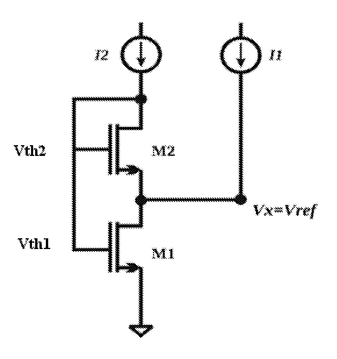
[0024]As can be inferred by the attached figures, the present invention consists of using a SCM (Self Cascode MOSFET) structure composed of two transistors with different threshold voltages (Vth). Furthermore, both transistors are biased with two independent current sources, I1 and I2. These bias currents are still relatively small and within the range of a few nano Amperes (nA), that results in a substantially low power consumption. As can be seen in FIG. 1, the proposed SCM structure has the M1 transistor as an NMOS transistor which has its threshold voltage (Vth1) larger than the threshold voltage of the M2 transistor (Vth2), so Vth1>Vth2. The bulk (b) terminal of both transistors is connected to the ground terminal, so the M2 transistor has a body effect (Vbs≠0).

[0025]The SCM structure basically consists of two NMOS transistors, M1 and M2, connected so that the M2 source electrode is tied to the M1 drain electrode. The M2 drain electrode is connected to the M2 and M1 gate electr...


PUM


Abstract

A simple SCM (Self Cascode MOSFET) structure to generate a sub-1V reference voltage in the SCM intermediate node. The structure requires only 2 transistors to create a temperature-compensated reference voltage. When sized correctly, the transistors in the SCM will operate both at weak, moderate or strong inversion, and in the saturation region or saturation and triode regions, providing good correspondence and low part to part variation. The following proposal innovates by operating with supply voltages on a broad variation range, from 3.6V through below 1V (sub-1V operation), with bias currents in the range of tens of nA (nano Amperes) and temperature variation smaller than ±1% from −40° C. through 85° C. This is an extremely low cost implementation (in terms of area and complexity), compatible with standard CMOS manufacturing processes, and very robust (in terms of fab-to-fab transference, technology mapping, and also well controlled part-to-part variation).

Description

FIELD OF THE INVENTION[0001]Generally, the present invention belongs to the technological field of electronic systems and more specifically refers to reference voltage circuits.BACKGROUND OF THE INVENTION[0002]The technologies concerning the development and manufacturing of semiconductors have advanced exponentially. Nowadays, the processed transistors have diminished in size and area of an integrated circuit (IC). This is an extremely important fact since a greater range of devices and integrated circuits can be employed and implemented, providing the possibility of adding more functions to a single chip, thus reducing the required area and power consumption.[0003]Reference voltage circuits are essential blocks for the development of analog and mixed signal blocks such as voltage regulators, AD converters, flash memories, DRAM memories, switched capacitor circuits, RF communication blocks, comparators, etc. The power required by advanced systems has achieved increasingly low and ti...

Claims


Application Information

Patent Timeline
IPC IPC(8): G05F1/46
CPCG05F3/24G05F1/468
Inventor PORRAS, FERNANDO CHAVEZOLMOS, ALFREDOMARTINEZ BRITO, JUAN PABLO
Owner CENT NACIONAL DE TECHA ELECTRONICSA AVANCADA
Why Eureka
Try Eureka